Download
1 / 21
210 likes | 232 Vues
Discover the unprecedented opportunities in semiconductor technology for high-energy physics, astrophysics, and more. Explore the advancements in detector scale, resolution, and functionality. Learn about enabling R&D and the application-specific capabilities of semiconductor detectors. Dive into the future of 3D electronics and the possibilities it offers for precise tracking and imaging.

E N D
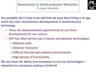
Revolutions in Semiconductor DetectorsR. Lipton (Fermilab) • You probably don’t have to be told that we have been living in an age which has seen revolutionary developments in semiconductor technology • There are unprecedented opportunities to use these developments for our science • HEP has often led the way in device and detector technologies • Detector scale • Detector resolution • Difficult thermal and radiation environments • High density of functionality • We also have the ability and motivation to try new technologies – important to companies seeking a foothold.
Detector Commandments • Thou shalt minimize mass • Thou shalt have high bandwidth • Thou shalt be radiation hard • Thou shalt not dissipate power • Thou shalt have complex functionality • Thou shalt not bear false witness (good resolution) • Thou shalt not kill (no dead regions) • Thou shalt not covet thy neighbors signals (minimize crosstalk) • Honor thy funding agencies (keep costs down) • …
Palette of Future Detectors Neutron fluence/cm^2/bunch • ILC Vertex Detector • Superb impact parameter resolution • Transparency, low power • Muon Collider • All requirements for the ILC plus … • Substantial detector and radiation backgrounds • CLIC • ILC + few ns time resolution • SLHC • 200-400 int/25 ns crossing • Triggering and data flow • Intensity Frontier • Precise timing, fast response • Low mass, precise tracking • Astrophysics • High mass semiconductor arrays for dark matter • Imaging detectors for focal planes
Enabling R&D SVTC • There are a few circumstances that have enabled these opportunities • Silicon (and other semiconductor) foundries which can offer specialized processes • Design tools which model semiconductor physics in detail • ASIC design tools • Companies offering specific processing and interconnect services • University Nanofabrication facilities • Collaborations to share costs
Application Specific Semiconductor Detectors • In many cases we can now tailor a device to an application. The palette includes: • Material • Silicon • Epitaxial (thin deposited layers), float zone, magnetic Czochralski • Ge, SiC, GaN, Diamond, carbon nanotubes, organic semiconductors …. • Structure • Epitaxy, SOI, MAPS • Wafer bonding • Nanofabricated structures • Implantation • Pixel structures (capacitance) • Multiple wells • Charge manipulation and storage (CCD, silicon drift) • Charge collection • Diffusion (slow, CMOS MAPS) • Drift – design for optimal fields (Arai) (Fillfactory) (KEK)
Solving Problems - MAPS MAPs – technology used in cameras using charge collection by diffusion in a thin(~5 mm) epitaxial layer Slow-charge collection by diffusion Low S/N Charge lost to parasitic PMOS Thick, high resistivity epitaxial layers 4 Well process 3D assemblies Fully depleted substrates (RAL) (IPHC-DRS) Thinning and backside processing (IPHC-DRS)
Example-SOI Fe55 40mm 20mm • An SOI device contains a thin (200nm) silicon device layer mounted on a “handle” wafer. Handle can be a high resistivity detector. • First studied in 1993 by CERN/CPPM/IMEC • 2000s Crakow group in-house fabrication • FNAL SBIR studies with American Semiconductor dual gate transistors • Detector-only wafer • KEK-organized multiproject runs with OKI • Excellent foundry-FNAL communication • Physical models to understand digital-analog crosstalk • Cornell - device simulation • Parallel work on thinning/backside process • Qualification of 3M thinning process • Development of laser anneal process (FNAL-Cornell)
More complex architectures • Nested well shielding implants for SOI and CMOS devices • Reduce digital-analog coupling and backgate effects • INMAPS quad well process (RAL) • ISIS concept – mate CCD and CMOS processing technologies • SPT Gigapixel tracker • Detailed process simulation and close collaboration with foundries crucial
3D Electronics • Industry and government initiatives to develop “vertical integration” as it was recognized that scaling feature size would not extend Moore’s law beyond ~ 2020 • The 3D technology development program has provided new sets of capabilities: • Wafer bonding • Sensor/readout integration • Etching and processing of precision vias in silicon • Fine pitch interconnect • 3D and edgeless sensor technology • Precision alignment • Wafer thinning • Low mass sensors • Backside processing • New ways to think electronics/detector integration. Capabilities are accessible now Tezzaron 2-tier wafer MIT-LL Three tier SOI wafer
Interconnections Cu-Cu Adhesive (Tezzaron) Oxide (RTI) (Ziptronix) Cu-Sn Indium (T-Micro) (IZM)
3D Applications • We are just at the beginning of exploring 3D • FNAL Tezzaron/Chartered + KEK/OKI + Future • 3D sensors (S. Parker et al) • ILC Vertex • LHC track trigger • X-ray imaging with time tag • CMOS pixel with PMOS devices placed on the tier without sensing diodes • ATLAS pixel chip size reduction • Super B vertex • X-ray imaging • B factory Vertex • CMOS/CCD integration • SiPM with per pixel digital readout • 3D associative memories for triggering VIP2 Chip
3D Examples sensor interposer VICTR 3D Chip Oxide bonded • CMS Track trigger • Need to correlate hits from 2 layers separated by ~mm to filter on pt > 2-3 GeV • 3D allows connection of chip to both top and bottom sensors space by low density interposer • Correlations formed locally by bottom chip, saving power, complexity • Fast 3D associative memories for triggering • Arrange multi-tier memory to correspond to tracking layers • 4-side buttable edgeless imagers (MIL-LL) sensor 70 micron 3D imager pixels 5 layer ADC/control Connector
Multiproject Collaborations KEK-OKI Reticule Fermilab/Tezzaron 2 tier CMOS 3D reticule MIT-LL 3 tier SOI 3D reticule
Nano-Injectors(Northwestern U.) • Combination of semiconductor near IR detector and nanofabricated electrodes • Hole is generated in the bulk and drifts/diffuses to the injector • Drift to 50 nm high and 100 nm wide diameter nanoinjector • Low capacitance of the node -> single hole can lower the potential barrier enough to transfer stored charge. Single hole creates an effective charge density of more than 400 C/m3. • Non-avalanche charge gain(10k) with noise lower than shot noise
Thick detectors • Independently process complex top and bottom readout wafers • Use thick material from boules as sensor region • Wafer bond to readout electronics • This eliminates some of the constraints on device thickness due to processing equipment • Dark matter detector? • - Process developed at NRL
Very Thin Trackers • What is the thinnest “practical” silicon tracker? • Noise – Increasing gm costs power (gm~Id), minimize Cdet->pixels ~ 10 ff possibleminimal coupling to other electrodes • Power – assume id=500 na, pitch 25 microns • Signal – shoot for 25:1 s/n • 80 e/h pairs/micron • Speed – let’s say 5 ns • Mechanical – • Can thin to ~10 microns 25 micron pixel pitch 12 micron implants 5 ns shaping Cdet only 500 na FE transistor current (IEEE V41(2) p397) Electronics and interconnect dominant Oxide bond DBI Interconnect 20mm 50mm
Power • Power distribution will be a major challenge in future experiments • Underestimated in LHC experiments, ~60% of power dissipated in cables • Power pulsing in ILC experiments peak current ~100-200 x average current • Low voltage operation -> high current • Cable mass is unacceptable -> serial powering or DC-DC conversion • Need high voltage, low loss, radiation hard power conversion. (Yale) • DC-DC near Load Losses > I2 x R • Silicon ÷10 I Reduction: Power Losses reduced by 100 • GaN ÷ 50 I Reduction: Power Losses reduced by 2500 – lower resistive, joule losses, rad hard
Electronics and ASICs • ASICs are now at the heart of most experiment systems • Expertise is scarce and expensive • Tools are costly for labs (mostly cheap for universities) • Run at full speed to keep up with changes in technologies, design requirements … • Need a “team” with varied expertise to be most productive • Laboratory groups • Collaboration with university EE Depts. • Inter-laboratory collaboration • Need to utilize multiproject runs to contain costs • Testing is crucial and complex • Wafer probing • Functional testing (stimulus systems) • Radiation testing • Beam tests
Future Opportunities • Cheaper, large area devices for (particle flow) calorimetery • Printed semiconductors • Large area high energy density (calorimeters) • Flexible geometries • Thinned, flexible sensors • Organic semiconductors • 103 too slow?, large bandgap • Hydrogenated amorphous silicon • Laser annealed? SOI-based from American Semiconductor Flexible image sensor array with bulk heterojunction organic photodiode Flexible a-Si:H sensor array fabricated at 150 °C, patterned by ink-jet digital lithography on PEN
Getting Involved • A healthy national R&D program requires involvement at many levels • National labs can provide • Test beams • Engineering support (especially ASIC) • Major equipment • Coordination • Universities can provide • Design and physical simulation • Sophisticated software often cheap or free to universities • Testing using students and postdocs • Contact with Nanofabrication faculties • Students can often do “hands on” work • Range of unique capabilities designed as user facilities
Conclusions • Vast range of R&D Opportunities in semiconductor detectors • Integration detectors and electronics • Extremely thin detectors • Mating of heterogeneous detector types • “Application Specific” designs • Integration of detectors with nanotechnology • Vertical integration of electronics and sensors • Collaboration is essential • The only way to afford silicon fabrication • Close collaboration with industry to develop technology • Software, expertise, lab capabilities are distributed among laboratories and universities.