Download
1 / 21
230 likes | 274 Vues
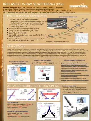
Explore the current status and opportunities of Inelastic X-ray Scattering (IXS) at NSLS-II workshop. Learn about the scientific missions of the project beamline, specifications, and requirements for high-resolution experiments. Discover the optical scheme and overall layout for achieving 0.1 meV resolution at 9.1 keV.

E N D
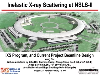
Inelastic X-ray Scattering at NSLS-II IXS Program, and Current Project Beamline Design Yong Cai With contributions by John Hill, Xianrong Huang, Zhong Zhong, Scott Coburn (NSLS-II) Alfred Baron (RIKEN), Yuri Shvyd’ko (APS), Alex Babkevich and Nigel Boulding (Oxford-Danfysik) IXS@NSLS-II Workshop, February 7-8, 2008
IXS: Current Status • A powerful (but weak) probe offering energy and momentum resolved information on dynamics and excitations in condensed matter systems • Practical applications with highly successful state-of-the-art implementation at ESRF, SPring-8 and APS • Broad areas of applications, including but not limited to the followings: • Lattice dynamics – Phonons in solids, vibration modes and relaxation processes in disordered systems: routinely operational at ~1meV resolution with ~109 photons/sec at ~20keV using symmetric backscattering crystal optics • Charge dynamics – Plasmon in simple metals, complex electronic excitations in strongly correlated systems: best resolution at ~50meV with ~1011 photons/sec at ~10keV for the most demanding experiments • Element specific applications – Chemistry and materials science, materials under extreme conditions of pressure and temperature: x-ray Raman scattering, x-ray emission and absorption spectroscopy by partial fluorescent yield at low resolution (~300meV or lower)
IXS Opportunities at NSLS-II • Key scientific drivers identified thru community inputs (CDR, user workshops) • 0.1-meV scientific case: filling the gap between high and low frequency probes • Visco-elastic crossover behaviors of disordered systems and fluids • New modes in complex fluids and confined systems • Collective modes in lipid membranes and other biomolecular systems • 1-meV scientific case: • Relaxation processes in disordered systems (glasses, fluids, polymers …) • Phonons in single crystals, surfaces, thin films, high pressure systems, small samples • Exotic excitations in strongly correlated systems • 10~50-meV (including lower resolution) scientific case: • Non-resonant and resonant inelastic scattering on charge dynamics • X-ray Raman scattering, x-ray emission and absorption spectroscopy by partial fluorescent yield combined with small beam for small samples of micrometer scale, high pressure, high fields, low and high temperature … • High flux experiments with low(er) energy resolution
Scientific Mission of the Project Beamline • Develop advanced instrumentation that enables IXS experiments at extremely high resolution of 0.1 meV at ~10 keV – a key goal for NSLS-II. • Why 10keV, as opposed to 20keV or higher? • Technical merits: higher brightness and flux for NSLS-II • Scientific merits: better momentum resolution for a given solid angle, or the same momentum resolution for larger solid angle • Counting efficiency: a complex issue, sample and optics dependent, requirecareful evaluation • Possible scheme based on highly asymmetric backscattering optics proposed by Yuri Shvyd’ko working at 9.1keV, require considerable R&D(more from Xianrong Huang and Zhong Zhong’s talks) • What are the alternatives?
Specifications and Requirements • Radiation source • Provide flux > 1010 phs/s/0.1meV at 9.1 keV, to provide > 109 phs/s/0.1meV at sample, require beamline overall efficiency > 10% • Essential source size and divergence stability, vibration and thermal stability for achieving the 0.1meV resolution (more from XianRong Huang’s talk) • Beamline and Endstations • Two end stations, one with 0.1meV and the other with 1meV resolution • Primary beam energy at 9.1 keV to match scheme for achieving 0.1meV resolution • Beam energy tunable over 7~12 keV for added flexibility (e.g., other refractions) • Energy scan range: order of 0.1 ~ 1eV, appropriate for the excitations to be studied • Momentum resolution: 0.1 ~ 0.4nm-1 at 9.1keV • Momentum range: up to 80 nm-1 to cover typical BZ sizes, ~120º at 9.1 keV • Spot size: ≤ 10 μm (H) x 5 μm (V), required for high pressure experiment • Sample environments: crystal alignment capability, handling of small samples of micrometer scale, high pressure, low and high temperature (4-800K), …, etc.
Overall Beamline Layout R-wall: 28.3m Walkway: 60.8m Beamline occupies a high-β straight section KB HRM KB VFM VCM HRM DCM • 1.0meV Endstation* • CDDW HRM (0.7meV) • CDW Analyzers (0.7meV) • larger q range (~80nm-1) • * (not in the project scope) • 0.1meV Endstation • CDDW HRM (0.1meV) • CDW Analyzers (0.1meV) • 0.1nm-1 q resolution • limited q range • FOE • HHL DCM • VFM / VCM
Optical Scheme for 0.1meV • CDDW mono to achieve 0.1meV with ~100µrad angular acceptance • Multilayer mirror to achieve 5~10mrad angular acceptance for CDW/CDDW analyzer Δθe = ~ 5μrad E = 9.1keV for Si(800) ΔE = 0.1 meV, φ = 89.6° Si(800) Side view Si(111) Si(220) < 5:1 focusing ~100μradacceptance ~20μrad divergence Si(800)
Multilayer Mirror for Analyzer • Requirements: • 100:1 demagnification (from 10mrad to 0.1mrad) • 10mrad angular acceptance • Greater than 50% efficiency • Possibility for parallelization of data collection E = 9.1 keV ~10 cm CDDW analyzer with ~0.1mrad acceptance We hope the beam here is a slightly focused beam with divergence ~0.1mrad and beam height ~50 µm We hope the mirror length to be ~10 cm. It can be either a (1) laterally graded multilayer or (2) a parabolically / elliptically bent periodic multilayer
Conceptual Beamline Layout • Multilayer mirror with 100:1 demagnification to provide 10mrad (vertical) angular acceptance for analyzer ~10m arm length
Experimental Floor Layout 25m BM line ~53m • Space may be sufficient for only one end station based on current scheme and 10mrad angular acceptance for analyzer • Another ~8m may be required for a second end station with 5mrad angular acceptance for analyzer, space for mirrors and phase plates ~61m + 2m (possibly) ID line
Insertion Device • U20 (IVU), or U14 (SCU) on a high-β straight section Figure of Merit: Flux / meV – provide flux > 1010 phs/s/0.1meV at 9.1 keV * U20: baseline device
Insertion Device Optimization • Optimize to maximize flux at 9.1keV: magnet period vs length vs minimum gapUntil superconducting devices become an option, the U20-5m seems to be the best option
Extended Long Straight • It is possible to obtained one 15m extended long straight by extending one 9.3m high-β straight and shortening two adjacent 6.6m low-β straights of the current lattice • Preliminary solution indicates that it would be possible to put in two U20-5m devices with refocusing magnet. Potentially more than triple (3.38 times) the flux compared to one U20-3m baseline device • There are accelerator issues (tune shift compensation, radiation shielding) and cost impact. βx = 18.5, βy = 3.5 for extended LS βx = 0.8, βy = 0.8 for short straights
Straight Section • High-β straight section (9.3m) is required for a long device • Additional benefits associated with a high-β compared to a low-β straight section : • Bigger horizontal source size but smaller horizontal divergence, leading to smaller horizontal photon beam size shorter horizontal mirrors • Lower power load within the central cone of the photon beam delivered to the first optics heatload is more manageable for first optics, even for two U19 undulators. • Important: Flux within the central cone remains the same! Photon beam size and power (one U19, at 9.1keV) thru angular aperture of 4s(H)x4s(V).
First Optics Enclosure (FOE) • DCM: cryogenic cooled Si(111). • FEA analysis on first crystal of DCM shows < ±5 µrad slope error at 115W heat load • Forhigh-β straights, thermal effect would be less a problem (lower heat load). Cooled flu. screen DCM White beam & Bremsstrahlung stop Quadrant BPM Bremsstrahlung collimator Blade BPM White beam slit VFM Diamond window Cooled fixed mask
Beamline Collimating and Focusing Optics • Supplied by SESO • Multiples of 150mm in length • Each segment can be bent independently (2 electrodes for cylindrical and 4 electrodes for elliptical) • Bimorph can in principle correct its own tangential polishing slope errors and also correct for tangential errors introduced by other optics • KB bimorph pair can in principle correct for sagittal and tangential errors • Small beam size allows short mirrors with small incident angle (2.5mrad) and Si substrate for high reflectivity at 9.1keV • Candidate: Bimorph mirrors
0.1meV Endstation Layout • Features • Pre-focusing (up to 5:1) to reduce length of collimator (C) crystal for 0.1meV HRM • KB mirrors after HRM for micro focusing to ≤ 10(H) x 5(V) μm2 • Temperature scan of energy transfer • Analyzer(s) based on the CDW or CDDW scheme with multi-layer focusing mirror(s) to achieve 10(H)x5(V) mrad2 angular acceptance • High (0.1nm-1) momentum resolution in forward scattering, limited scan range • Extremely clean energy resolution function
1meV Endstation Layout • Features • Pre-focusing (up to 2:1) to reduce length of collimator (C) crystal for 0.7meV HRM • KB mirrors after HRM for micro focusing to ≤ 10(H) x 5(V) μm2 • Temperature scan of energy transfer • Analyzer(s) based on the CDW or CDDW scheme with multi-layer collimating mirror to achieve 10(H)x5(V) mrad2 angular acceptance • Large momentum scan range (up to 80nm-1) for single crystal studies, require phase plates • Extremely clean energy resolution function A natural step in achieving 0.1meV resolution
Schedule Summary • 2008~2011: Design phase, interaction with BAT, actively pursue 0.1meV R&D • 2011~2013: Construction phase, long lead-time procurements to begin in final design stage • 2014: Integrated testing phase, to be ready to take beam
Outstanding Issues • Multiple undulators on extended straight for more flux (depends on AS design)tuning compensation for beam dynamics, heat load on second undulator, cost impact • CDDW scheme to achieve 0.1meV HRM: Substantial R&D effort required (proof of scheme by end 2010, final design phase) • Multilayer mirror to achieve 10mrad angular acceptance for CDW / CDDW analyzers: (proof of scheme by early 2010, preliminary design phase) • Risks with current approach and mitigation strategies:1meV is promising, 0.1meV remains a major challenge, aggressively pursue the R&D and seek alternatives • Possibility to combine two end stations into one: energy resolution tuning • Parallel data collection: multiple analyzers, area detector Your inputs are important!