Inelastic Scattering - Introduction
Inelastic Scattering - Introduction. Quasiparticle Property Measurements. Two reasons why we can generate and detect:

Inelastic Scattering - Introduction
E N D
Presentation Transcript
Quasiparticle Property Measurements Two reasons why we can generate and detect: 1) Since the fast electrons passing through a material can createplasmons, phonons, magnons, etc., i.e, signal generating, their resulting energy-loss electrons (used for signal detecting) carry the information of their properties. 2) Every electron that scatters off the same quasiparticle mode picks up the same scattering phase. - if an electron scatters off the quasiparticle, this electron carries information about the quasiparticle. e.g., the phonon gluing Cooper pair electrons together to make the superconducting fluxon.
Inelastic Scattering - Introduction We will focus on the collective interactions produced by inelastic scattering since no new information concerning x-rays and secondary electrons is available in Williams and Carter.
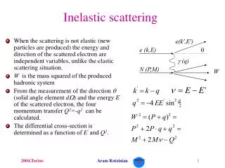
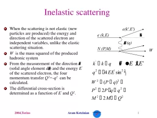
Electron Energy Loss Spectrum (EELS) Elastically scattered electrons – Bragg diffracted and diffuse elastically scattered electrons Zero-loss + phonon loss Low-energy, diffuse inelastically scattered electrons , I (Bulk Plasmons) (Surface Plasmons) (excitons, bandgap, dopants, defects) , E 000 beam Diffracted beam EELS spectrum of elastically & inelastically scattered electrons
Zero-loss & Phonon-loss Intensities for GaAs Aplanatic STEHM required total Intensity Zero-loss atomic planes 444 222 666 Phonon-loss s (1/Å) 0 10 20 f (mrad) Similar intensity loss for plasma loss electrons Doyle and Turner Acta Cryst. (1968). A24, 390
Plasmons and Phonons (next slide) * * for bulk plasmons, which exist inside the material. There is also a surface plasmon, which can be delocalized on the surface and exist for micro-seconds Longitudinal Waves Recall: the electron emitted from the source is a transverse wave.
Bulk Plasmons If the specimen is >100 nm, then another bulk plasmon can be created. The diffracted beams can also produce bulk plasmons.
Surface Plasmons The surface plasmon energy is equal to the bulk plasmon energy (10s of eV) divided by square root 2. For some specimen and certain conditions, surface plasmons can have a high intensity, e.g., gold nanoparticles, carbon nanotubes, etc., anything where the surface dominates over the volume of the specimen. Their creation by the electron beam creates a high intensity of surface plasmon loss electrons.
Plasmons 1. Localized Surface Plasmons Surface Plasmon 2. Propagating Surface Plasmons
Localized Surface Plasmons Simple semi-classical model: electron wave Surface plasmon densities around differently shaped nanoparticles A.J. Haes, C.L. Haynes, et al, MRS BULLETIN, 30 368 (2005)
Surface Plasmon Polariton The smaller the wavelength of surface plasmon, the shorter length it travels or propagates over the surface! H.A. Atwater, S. Maier, et al, MRS BULLETIN, 30 385 (2005)
Interband and Intraband Loss Electrons plus the presence of dopants and defects (electronic and photonic defects) in the band gap
Elastically & Inelastically Scattered Electrons Elastically scattered electrons – Bragg diffracted and diffusely scattered Zero-loss + phonon loss , I (Bulk Plasmons) (Surface Plasmons) (excitons, bandgap, dopants, defects) , E 000 beam Diffracted beam
The mean is and the half-width is . The Lorentzian distribution has very extended wings and is not defined as the integral is unbounded! What is the better electron source that represents elastically and inelastically scattered electron coming from material specimens? Lorentzian: Represents electrons from specimen that have lost energy such as inelastically scattered electrons including plasmon loss electrons and phonon loss electrons. Gaussian: Represents electrons from electron emitter plus Bragg diffracted beams, which have no energy loss. Gaussian Lorentzian
Primary Beam Lateral coherence enables continued interfere of beams as they are separated by changing voltage on electron biprism. New position on source, RS’1 and RS’2 enable the source size, shape and coherence to be determined. Perhaps, first time to measure properties of electron source coming from specimen. Condenser Aperture ac Crystal Specimen RS’1 RS’2 2qB Apparent Sources, Rs’ (virtual sources) Electron Biprism ( ) aB Main Beam Diffracted Beam Region 1 Region 2
Fringe Contrast versus Beam Separation 86V 82V The Lateral spatial coherence, do, is given as a function of electron source size, Rs, to be: a) b) 79V 74V 2 The reduced fringe contrast as the beams separate gives a measure of the shape of the electron sources. 1 2 c) d)
Beam Damage – Covalent & Ionic Materials * cathodoluminescence *
Surface Plasmon Polariton Propagating Surface Plasmons:Surface Plasmon Polaritons (SPPs) SPP are electromagnetic modes bound to metal/dielectric interface which propagates as a longitudinal wave along the surface. A.J. Haes, C.L. Haynes, et al, MRS BULLETIN, 30 368 (2005)
Sensor chip with gold film Advantages: Evanescent field interacts with adsorbed molecules only Coupling angle strongly depends on εd Surface Plasmon Bio Sensors (SPR-like experiment )
0.95 eV 0.78 eV Bandgap Engineering Figure 9: Energy band diagram versus lattice constant.