Download
1 / 17
180 likes | 393 Vues
Learn about SPICE models, typical conditions, and transistor characteristics for effective power dissipation analysis.

E N D
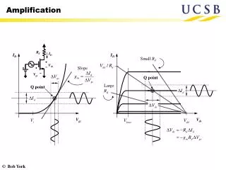
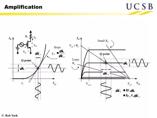
Rd ID Vds Vgs Amplification ID ID Small Rd Slope Q point Large Rd Q point Vgs Vds
Rd ID Vds Vgs Power Dissipation ID Imax Vmax Vds
CD4007 * CD4007 NMOS and PMOS transistor SPICE models * Typical - Typical Condition .model MbreakND NMOS + Level=1 Gamma= 0 Xj=0 + Tox=1200n Phi=.6 Rs=0 Kp=111u Vto=2.0 Lambda=0.01 + Rd=0 Cbd=2.0p Cbs=2.0p Pb=.8 Cgso=0.1p + Cgdo=0.1p Is=16.64p N=1 *The default W and L is 30 and 10 um respectively and AD and AS *should not be included. .model MbreakPD PMOS + Level=1 Gamma= 0 Xj=0 + Tox=1200n Phi=.6 Rs=0 Kp=55u Vto=-1.5 Lambda=0.04 + Rd=0 Cbd=4.0p Cbs=4.0p Pb=.8 Cgso=0.2p + Cgdo=0.2p Is=16.64p N=1 *The default W and L is 60 and 10 um respectively and AD and AS *should not be included.
2N7000 From DataSheet: (~2.5um technology) *2N7000 SPICE MODEL * .MODEL 2N7000 NMOS (LEVEL=3 RS=0.205 NSUB=1.0E15 +DELTA=0.1 KAPPA=0.0506 TPG=1 CGDO=3.1716E-9 +RD=0.239 VTO=1.000 VMAX=1.0E7 ETA=0.0223089 +NFS=6.6E10 TOX=1.0E-7 LD=1.698E-9 UO=862.425 +XJ=6.4666E-7 THETA=1.0E-5 CGSO=9.09E-9 L=2.5E-6 +W=0.8E-2) .ENDS * For large currents, Id-Vgs is approximately linear (dotted line) For small currents (<100mA) the behavior is parabolic
Subthreshold currents 2N7000
2N7000 Pdiss=400mW
Measuring Parameters gm, Vt • This is a simple method for estimating device parameters • Use diode-connected device (forces operation in saturation) • With an ammeter, vary the supply voltage until the desired bias current is achieved, and record the gate voltage Vgs • Adjust Vdd so that Vgs changes by a small amount (say 50mV), and record the resulting change in current • Continue varying the gate voltage until the current increases by a factor of 4. If the device follows a parabolic law, this means that the (Vgs-Vt) must have changed by a factor of 2 Vdd A Vout For r = 2:
Common Source Amps Vdd Vdd Rd Rd Rg1 Rg1 ∞ ∞ ∞ Rgen ∞ Vout Vout Vin RL Vgen Rg2 Rg2 Rgen gmvin gmvin Vin Rin vin Rout Vout Vgen Rin vin Rout RL
Lab Circuits +10 V +10 V 220 Ω 100 kΩ 220 Ω 10 μF Vout 100 kΩ 10 μF Vout 10 μF Vin 10 μF Vin 10 kΩ 10 kΩ Rg1 Rg1 100 Ω 10 μF
Common Source Amplifier Vdd Rd Rg1 ∞ Rsig ∞ Vout RL Vsig Rg2 Rs ∞
Vdd G D Rd ∞ gmvgs S D 1/gm ∞ Vout gmvin 1/gm vin S ∞ Vin G Id gmvin Vin 1/gm vin Rd Vout Common Gate Amplifier
Common-Gate Amplifier Vdd Rd Rg1 Vout Rg2 ∞ ∞ RL Rgen ∞ Vgen Rs Rgen gmvin Vgen Rin vin Rout RL
Lab experiment +10 V 220 Ω Rg1 10 μF 10 μF Vout 100 kΩ 10 kΩ Vin Rs 100 μF 100 Ω
Source Follower Vdd Rd Rg1 Rgen ∞ Vout ∞ Vgen Rg2 Rs RL
CS Resistive Feedback Vdd Vdd Rd Id Rf ∞ Rf ∞ Vout Vout ∞ ∞ RL Vin Vin Rg Rgen Rg gmvgs gmvin Vin vgs Rout Vout Vgen vgs RL
VDD 1 14 P P 2 13 3 12 4 11 P N 5 10 6 N 9 8 7 N VSS CD4007 14 2 11 13 1 6 3 10 12 8 5 7 4 9
Active Loading Vdd Vdd Q2 Q3 C2 Rf Vout C1 Q4 RL Q1 Vin