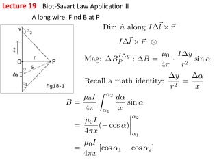
Lecture 19
Lecture 19. OUTLINE Common-gate stage Source follower Reading: Chapter 7.3-7.4. Diode-Connected MOSFETs. Diode-connected NMOSFET. Diode-connected PMOSFET. Note that the small-signal model of a PMOSFET is identical to that of an NMOSFET. Small-signal analysis circuit.

Lecture 19
E N D
Presentation Transcript
Lecture 19 OUTLINE • Common-gate stage • Source follower Reading: Chapter 7.3-7.4
Diode-Connected MOSFETs Diode-connected NMOSFET Diode-connected PMOSFET • Note that the small-signal model of a PMOSFET is identical to that of an NMOSFET Small-signal analysis circuit Small-signal analysis circuit
Common-Gate Amplifier Stage • An increase in Vin decreases VGS and hence decreases ID. • The voltage drop across RD decreases Vout increases • The small-signal voltage gain (Av) is positive.
Operation in Saturation Region • For M1 to operate in saturation, Vout cannot fall below Vb-VTH. Trade-off between headroom and voltage gain.
I/O Impedances of CG Stage (l = 0) Small-signal analysis circuit for determining input resistance, Rin Small-signal analysis circuit for determining output resistance, Rout
CG Stage with Source Resistance Small-signal equivalent circuit seen at input For l = 0:
The output impedance of a CG stage with source resistance is identical to that of CS stage with degeneration. Small-signal analysis circuit for determining output resistance, Rout
CG Stage with Biasing • R1 and R2 establish the gate bias voltage. • R3 provides a path for the bias current of M1 to flow.
CG Stage with Gate Resistance • For low signal frequencies, the gate conducts no current. Gate resistance does not affect the gain or I/O impedances.
CG Stage Example Small-signal equivalent circuit seen at input Small-signal equivalent circuit seen at output
Source Follower Stage Small-signal analysis circuit for determining voltage gain, Av Equivalent circuit
Source Follower Example • In this example, M2 acts as a current source.
Rout of Source Follower • The output impedance of a source follower is relatively low, whereas the input impedance is infinite (at low frequencies); thus, it is useful as a voltage buffer. Small-signal analysis circuit for determining output resistance, Rout
Source Follower with Biasing • RG sets the gate voltage to VDD; RS sets the drain current. (Solve the quadratic equation to obtain the value of ID.) Assuming l = 0:
Supply-Independent Biasing • If Rs is replaced by a current source, the drain current ID becomes independent of the supply voltage VDD.