Coherence in Superconducting Materials for Quantum Computing
Coherence in Superconducting Materials for Quantum Computing. David P. Pappas Jeffrey S. Kline, Fabio da Silva, David Wisbey National Institute of Standards & Technology, Electronics & Electrical Engineering Laboratory, Boulder, CO Collaborators Will Oliver, Paul Welander – MIT/LL

Coherence in Superconducting Materials for Quantum Computing
E N D
Presentation Transcript
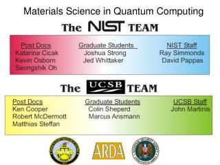
Coherence in Superconducting Materials for Quantum Computing David P. Pappas Jeffrey S. Kline, Fabio da Silva, David Wisbey National Institute of Standards & Technology, Electronics & Electrical Engineering Laboratory, Boulder, CO Collaborators Will Oliver, Paul Welander – MIT/LL Ray Simmonds, Kat Cicak, Josh Strong NIST, Boulder Matthias Steffen, IBM Watson Kevin Osborn, LPS, MD John Martinis, Haohua Wang, UCSB Rob McDermott, U of W Sponsors
The quantum computing challenge Implementations Photons Ion traps Neutral atoms NMR ~~~~~~~~~~~~~~ ~~~~~~~~~~~~~~ Spins in semiconductors Quantum dots ~~~~~~~~~~~~~~ Superconducting: ~~~~~~~~~~~~~~~ Charge Flux Phase Coupling Isolation Prepare Prepare Prepare Qubit Qubit Qubit Measure Measure Measure interact interact Decoherence: external – radiation, heat, acoustic… internal – materials, crosstalk…
Superconducting qubit measurement setup • Ante • Dilution Refrigerator • Low temperature, < 50 mK • RF measurement • Low power ~ 1 photon of energy in cavity • Improves coherence • Removes quasiparticles in superconductor • Reduces thermal radiation • Hurts coherence: • Low-energy, two-level excitations in amorphous materials
The Josephson Junction • Building block of superconducting quantum bits (qubit) • Josephson relations (’62, ‘73) 1.7 nm Al amorphous AlOX Al TEM photo • Not ohmic = > I periodic in d • Voltage only when phase is changing • System is nonlinear for high I
Logic Non-linear oscillator Excited |1> vs Ground state |0> Island Charged vs. Not charged Current circulation Left vs Right Types of qubits “Phase” “Charge” “Flux” You & Nori, Physics Today, November (2005)
Anatomy of a conventional superconducting circuitMaterials perspective Tunnel barrier Wiring Insulator Substrate Traditional
Conventional materials are usedfor a lot of really good reasons… • Si substrate with thermal amorphous a-SiOX on top • Smooth, standard lithography, inexpensive • a-SiOX insulators – CVD • Smooth (no pinholes), low T, easy • a-AlOX tunnel barrier – thermal or plasma oxidation • Smooth, no pinholes, low T, easy, self-limiting • Nb or Al wiring – sputter deposit, polycrystalline • Low temperature, smooth, relatively high TC Need strong motivations for change …
Short lifetimes of quantum information in solid state superconducting qubits Lifetime 0.5 T1 = 23 ns 0.25 Prob. |1> state 0 “Rabi” oscillation 200 100 0 Meas. delay (ns) • Relatively short lifetimes and operation cycles • Need lifetime/gate operation time > 1000
Outline • Electrical model of a phase qubit • Two Level Systems (TLS) as loss mechanism • substrate & insulators a-SiOX • tunnel barrier a-AlOX • Test structures for materials analysis • New directions in materials • Improved substrates a-Si & removal • Crystalline barriers Al2O3 • Recent progress
LCR electrical model for phase qubit LJ~sinf CJ~1-100 x10-12 Rjunction – non-linear QP tunneling - ? Rdielectric – bound dipole relaxation ~ ? Junction & insulators = G(V) Intensity What can we easily measure & optimize? • Quality factor – Energy stored/Energy lost/cycle • Q = = w0/Dw • T1 = Q/w0 • Delectric loss tangent: • tand = Im(e)/Re(e) • = 1/Q frequency
Loss in amorphous materials (SiOX-OH-) Schickfuss & Hunklinger, (1974) • Low energy displacements of dipoles, saturate at high T, P • Lose energy through phonon creation • tand = 3x10⁻³, Q ~333, T1~40 ns • Approaches: 1) Reduce or eliminate dielectrics 2) Optimize mtls. – e.gSiN, a-Si… ++++ ++++ E d _ _ _ _ _ _ _ _
Minimize & optimize dielectric - qubit Rabi oscillations Rabi oscillations > 600 ns !! Sapphire substrate + SiN insulator:
Optimized SiNx for coherent quantum circuits Kevin Osborn Group Loss Tangent for SiNx films SiNX pillar from high-stress film Qi=1,400 200 nm other labs: NIST, UCSB SiNX Qi=25,000 Al film smooth etch profile from HDP CVD film precursor ratio: N2/SiH4 = 1.8 x-ray reveals polycrystalline order stress = 600 MPa compressive Tgrowth = 300 C The loss tangent is sensitive to PECVD growth!
Optimize dielectrics with simple L-C circuits O’Connell, APL (2008) LC – parallel plate C CPW C Substrate L insulator Predicts:
Other approach – remove dielectricsSimmonds, Strong, Cicak et. al, NIST Boulder (2008) • Vacuum gap capacitor with an inductor => Flexible circuit - allows us to test the loss in a junction under identical conditions
Add a 1.5 nm, 10 mm2 a-AlOX JJ to the circuit • Generally understand dielectric problem – Improve & Reduce • Significant loss in the amorphous AlOX junction • 1.5 nm thick – very strong coupling • Focus on tunnel barriers
Tunnel barrier material characterizationQubit spectroscopy • Increase the bias voltage (tilt) • Frequency of |0> => |1> transition goes down Increase I bias Splittings
Splittingsin charge qubit - Cooper-Pair Box Z Kim et al., Physical Review B 78, 144506 (2008). 1 mm Al/AlOx/Al gate island junction Vg B gate island (Ec,EJ) Cg junction Vg B
Effects of splittings • Quench Rabi Oscilations – strong coupling to qubit • Reduces the measurement fidelity Spectroscopy Rabi oscillations
Origin of spectroscopy splittings • Individual, strongly coupled TLS’s in barrier • Distribution of excitation energies - amorphous AlOX 13 um2 junction 70 um2 junction • More splittings, small gaps • weak coupling • Fewer splittings, large gaps • stronger coupling Density of splittings~ 1/GHz/mm2 in 1.5 nm thick junction Reduce materials where possible Improve materials by eliminating TLS’s
1) Reduce materials where possible • Reduce size of junctions in qubits • increases f0 due to smaller capacitance • Add high quality external capacitor to bring f0 down (SiN, a-Si) Steffen, et. al PRL (2006) • T1 ~ 170 ns (SiN) & 600 ns (a-Si:H) • Factor of 2 shorter than expected - Still have a-AlOX in barrier
Epitaxial Re/Al2O3 Amorphous AlOX Epitaxial Al2O3 @ 800 C @ RT @ 850 C Al Re Al 10-6 Torr O2 4×10⁻⁶ Torr O2, Growth of single-crystal Al2O3 (sapphire) tunnel barrier • Rhenium bottom electrode: • Superconducting – TC ~1 K • hcp - lattice match Al2O3 • high melting T Polycrystalline Al @ RT
Al Re (2) Improve JJ’s with crystalline barriers - Al2O3 & MgO Al Al2O3 • Good - High sub-gap resistance • First high quality junctions made with epitaxial barrier • Fabricate into qubit Re(0001) 20 mK I-V curve V(mV)
Qubit with 25 mm2 epitaxial Al2O3 junction Kline, et. al, Supercond. Sci. Tech. 22, 015004 (2008) • T1 > 500 ns • best for SiO2 insulator & large junction • No external capacitance • Splitting density reduced • ~3-5 times lower than amorphous barrier of same area
12 Qubit Test Die Layout Qubit loop Bias coil DC-SQUID
Two level systems in junction Amorphous AlO tunnel barrier • Continuum of • metastable vacancies • Changes on thermal cycling • Resonators must be 2 level, • coherent with qubit! I
Design of tunnel junctions Existing technology: What we need: Amorphous Aluminum oxide barrier Spurious resonators in junctions Fluctuations in barrier No spurious resonators Stable barrier Top electrode Poly - Al Crystalline barrier a-Al2O3 Amorphous tunnel barrier a –AlOx – OH- SC bottom electrode Poly- Al amorphous SiO2 Low loss substrate Silicon
Q: Can we prepare crystalline Al2O3 on Al? 68 Metallic aluminum 10 Å AlOx on Al (300 K + anneal) 10 Å AlOx on Al (exposed at elevated temp.) AES Energy of Reacted Al (eV) Aluminum Melts Al in sapphire Al203 Annealing Temp (K) • Anneal the natural oxides • Oxidize at elevated temp. Binding energy of Al AES peak in oxide A: No – need high temperature bottom wiring layer
Motivations – New wiring materials • Conventional Al, Nb: • Surface oxides with spin polarized traps • 1/f flux noise, dephasing times, density ~ 1017/m2 • Alternative materials: • Re: resists oxidation, high melting T, hcp lattice => Al2O3, • Al passivated with Re or Ru => resists oxidation e- traps Kondo traps Coupled TLS Koch, Clark, di Vincenzo (PRL 2007) Faoro, Ioffe PRB (2007) McDermott, et. al (2007)
Improvement of junctionsseen in spectroscopy of 01 transition Epitaxial barrier 70 m2 Amorphous barrier 70 m2 T = 25 mK • Density of coherent splittings reduced by ~5 in epitaxial barrier qubits
Source of Residual TLFs: Al-Al2O3 interface? Al2O3 White is oxygen Oxygen content Distance (μm) • Electron Energy Loss Spectroscopy (EELS) from TEM shows • Sharp interface between Al2O3 and Re • Noticeable oxygen diffusion into Al from Al2O3 • Indicates presence of a-AlOx at interface • Will “heal” pinholes
Need to improve top barrier interface! • Interfacial effect • ~1 in 5 oxygens at Al interface • Agrees with reduced splitting density Al non-epi Al interface Oxygen ~1.5 nm a-AlOx epi-Re interface Re
Top electrode mattersAl top electrode always gives good I/V Al/a-AlO/Al Re/c-AlO/Al Re/c-MgO/Al Al top electrode Tunnel barrier Bottom electrode a: Amorphous c: Crystalline substrate Supports conclusion that Al top electrode “heals” pinholes
Re on top makes JJ leaky substrate Re/c-AlO/Re Re top electrode Tunnel barrier Bottom electrode => Pinholes in tunnel barrier
Goals • Inter-laboratory compatibility • Infrastructure - 6”-wafer chamber for epitaxial trilayers • Develop 6” substrate capability • Re/Al2O3/Al, Re/Al2O3/Re • Supply samples to flux qubit, 6” wafer fabrication facililty • Extend work on epitaxial tunnel barriers to flux qubits • Continue on barriers at chip level • Chip level • Develop JJ and qubit circuits compatible w/flux qubits • study fully epitaxial systems • Study new materials for wiring layers • Al/Ru capping with anneal • Push to understand flux noise and wiring surfaces
Other potential new insulators – from VLSI world? • “Medium” K dielectrics? • Si • SiN • Al2O3 • MgO • Diamond • ZrSiO • CaO • SiC • Need to use thicker insulators • “low” K dielectrics? • doped SiOx (F, C • Porous SiOx • Spin-on polymers (HSQ) new Probably not
tunnel barrier insulator wiring substrate New directions Materials Difficulties CMOS
Two-level systems in a-SiO2 Low E High E Low E SiO2 - Bridge bond Schickfus and Hunklinger, 1975 E d • TLS bath saturates at • high E (power), decreasing loss Amorphous material has all barrier heights present
Temperature Dependence of Q Q also decreases at low temperature! ~T RSiO2=2.1kW
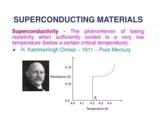
dissipation increases, by 10 – 1000! Problem - amorphous SiO2Why short T1’s in phase Josephson qubits? • Dissipation: Idea - Nature: • At low temperatures (& low powers) • environment “freezes out”: • dissipation lowers Change the qubit design: • find better substrates • find better dielectric & minimize insulators in design
Common insulator/substrate materials • SiOX • Bridge bond, unstable • Amorphous films have uncompensated O- , H, OH- • Si3N4 • N has three bonds – more stable • Amorphous films, still have uncompensated charges, H • 20% H for low T films, ~ 2% H in high T films • Al2O3 • Amorphous – high loss, similar to a-SiO2, has H, OH- in film • Single crystal (sapphire) - Very low loss system
Qubit has SiO2 Cap in || with J.J. & around lines Insert qubit pic here AlOx SiOX Stripline (C-SiOX ) Qubit L => Measure “Q” of simple LC resonators Josephson Junction (L&C)
Tunnel barrier materials Found improvements due to optimized materials in insulators Superconductor - Aluminum I Tunnel junction a- AlOx-OH-

