Exploring Nanometer-Scale Lithography Techniques
120 likes | 211 Vues
Learn about nanometer-scale lithography techniques like photolithography, electron beam lithography, and more for creating semiconductor devices. Discover applications and challenges in this presentation by Daniel Bernard and Benjamen Strobel.

Exploring Nanometer-Scale Lithography Techniques
E N D
Presentation Transcript
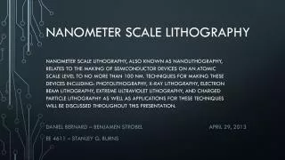
Nanometer scale lithography Nanometer scale lithography, also known as Nanolithography, relates to the making of semiconductor devices on an atomic scale level to no more than 100 nm. Techniques for making these devices including: photolithography, x-ray lithography, electron beam lithography, extreme ultraviolet lithography, and charged particle lithography as well as applications for these techniques will be discussed throughout this presentation. Daniel Bernard – Benjamen StrobelApril 29, 2013 EE 4611 – Stanley G. Burns
Topics to be covered Applications Memory Small integrated circuits Silicon Wafers Techniques • Photolithography • X-ray Nanolithography • Electron Beam Direct-Write Lithography • Extreme Ultraviolet Lithography • Charged Particle Lithography
Photolithography Also known as optical lithography, photolithography is a technique for patterning various surfaces and has the capability of producing sub patterns up to 100 nm with small wave lengths. Optical nanolithography requires the use of liquid immersion and resolution host. Most experts feel that optical nanolithography techniques are most cost effective than traditional methods of lithography. Image from: Huff
X-ray Nanolithography Another type of nanolithography is the x-ray nanolithography which is quite different from traditional x-ray lithography. It has the ability to improve and extend optical resolution of 15 nm by using short wavelengths of 1 nm for the illumination. This method is commonly used for batch processing. Image from: Wikipedia
Electron Beam Direct-Write Lithography Used for creating memory cells and sub patterns on the range of 7-40 nm sizes. The process includes emitting a beam of electrons in a pattern across a surface covered in a thin film called a resist (McCord). This “develops” the resist by removing either exposed or non-exposed regions. This resist can then be applied to substrate materials via etching to manufacture integrated circuits. Image from: West Holland
Electron Beam Direct-Write Lithography The images on the right show two different 22 nm SRAM patterns with different resists. The resist’s properties can change the way the electron beam interacts with it as shown on the right. The first image is created by the XE151B resist, and has a high resolution and contrast, whereas the second image, created using the XE15CB, shows lowered contrast, but higher sensitivity. Images from: Microelectronic Engineering
Extreme Ultraviolet Lithography (EUV) Considered a next generation technique for lithography. It uses a wavelength of light in the ultraviolet spectrum that should produce designs of about 13nm (Wikipedia). In order to produce EUV, A technique much the same as Electron beam is used only, cations must be used. Because cations can only be used in hot plasmas, the power requirement for EUV approaches more than 10kW (Harilal). UEV requires the system to be in vacuum (Wikipedia). Image from: Nikon
Applications at Nikon Examples shown for use by Nikon: DRAM Flash Memory Image shows a scale of progression of Nikon’s lithographic creations using EUV lithography variations. Image from: Nikon
Conclusion • Nanolithography isthe process of imprinting nanometer scale patterns on a substrate, often silicon wafers. • The aforementioned techniques are the future of nano-scale circuitry and memory. • Nanolithography is used to create memory cells and small integrated circuits. • There are still challenges including the immense amount of power required for EUV techniques.
REferences Michael Huff, (2002) "MEMS fabrication", Sensor Review, Vol. 22 Iss: 1, pp.18 - 33 "Evaluation of direct patternable inorganic spin-on hard mask materials using electron beam lithography." Microelectronic Engineering 98 (2012): 226+. Academic OneFile. Web. 25 Apr. 2013. Anonymous. Xrl currents3.gif. Wikipedia. <http://en.wikipedia.org/wiki/File:Xrl_currents3.gif>. McCord, M. A.; M. J. Rooks (2000). "2". SPIE Handbook of Microlithography, Micromachining and Microfabrication. Harilal, S. S.; et al. (2006). "Spectral control of emissions from tin doped targets for extreme ultraviolet lithography". J. Phys. D 39 (3): 484. Extreme ultraviolet lithography. 21 April 2013. Wiki. 25 April 2013. Holland, West. Mapper Lithography . West Holland. 2012. <http://www.westholland.nl/newsletter/custom_images/Mapper_klein.jpg>. Nikon. Figure 3. A generic EUV system.The Nikon eReview. 2013. Web Article. <http://www.nikonprecision.com/newsletter/fall_2008/article_05.html>. Nikon. Figure 5. The Nikon EUVL development roadmap. The Nikon eReview. 2013. Web Article. <http://www.nikonprecision.com/newsletter/fall_2008/article_05.html>.
Key Concepts • The most common techniques of nanolithography include photolithography, x-ray lithography, electron beam lithography, and extreme ultraviolet lithography. • Applications of nanolithography include memory cells and integrated circuits. • Different resists and masks can be used to change the contrast or sensitivity of a charged beam. • Commercial applications of flash memory have been produced at 25 nm (Nikon). • Some methods of nanolithography require large amounts of power, such as EUV nanolithography (sometimes around 10 kW of power).