Download
1 / 8
90 likes | 391 Vues
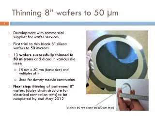
Thinning 8” wafers to 50 µ m. Development with commercial supplier for wafer services First trial to thin blank 8” silicon wafers to 50 microns 13 wafers successfully thinned to 50 microns and diced in various die sizes: 15 mm x 30 mm (basic size) and multiples of it

E N D
Thinning 8” wafers to 50 µm • Development with commercial supplier for wafer services • First trial to thin blank 8” silicon wafers to 50 microns • 13 wafers successfully thinned to 50 microns and diced in various die sizes: • 15 mm x 30 mm (basic size) and multiples of it • Used for dummy module construction • Next step: thinning of patterned 8” wafers (daisy chain structure for electrical connection tests) to be completed by end May 2012 15 mm x 60 mm silicon die (50 µm thick)
Next steps – Rockwood thinning • Sent 8 wafers back to Rockwood to be removed from tape with pick-and-place machine • ~70 pieces 15 mm x 30 mm and ~ 24 pieces 15 mm x 60 mm available • Prepare for building dummy modules as discussed with WG4 (mechanics, bus cables, glue) • Prepare layout for “intelligent dummies” (Antoine) • Purchase blanks (specs as Tower/Jazz wafers without epi layer) • DBG (dice before grinding) will used for next thinning trials.
Hybrid Dummies • First assemblies delivered from IZM • 8 single chip assemblies • 2 ALICE type ladders • Chip thickness: 50 um • Sensor thickness: 100 um • ALICE pixels 50 um x 425 um
Next steps - IZM • Measure thickness of elements (SEM, metrology) • Invesitgate bow of assemblies (though no real components!) • Send for 3D X-ray one assembly • Few more assemblies in pipeline at IZM