Download
1 / 22
220 likes | 327 Vues
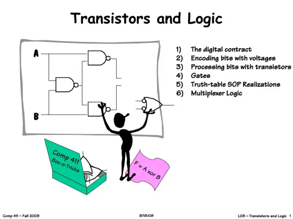
Learn about constructing gates with transistors, detecting the transistor bleed-through problem, connecting to power and ground, measuring outputs, using LED indicators, and the benefits of NANDs or NORs in logic operations.

E N D
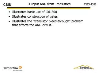
3-Input AND from Transistors • Illustrates basic use of IDL-800 • Illustrates construction of gates • Illustrates the “transistor bleed-through” problem that affects the AND circuit.
V+ A B C Out Transistors in Series • Construction of 3-Input (A,B,C) AND from transistors. • Note the resistor and output are at the “bottom”. • Three inputs (from switches)
V+ A B C Out Connection to Power Next slide shows the connection to power. + 5 volt power supply. Connects to top transistor
V+ A B C Out Connection to Ground After output. Through the current-limiting resistor.
V+ A B C Out Connection to Logic Switches • Switches connect to each transitor. • Switches are either: • 0-off, no voltage, • or 1-On, +5 volts
V+ A B C Out 2.13 Measuring Output with the Meter • Digital Volt Meter connects to output, and to the ground. • It measures the voltage differential between those two points.
Measuring Output with a LED The output can be connected to a Light Emitting Diode (LED) rather than to the DVM. A voltage of around 2.5 and greater will cause the LED to light. The LED is already wired on one end to the ground. A current limiting resistor ensure that the LED does not receive too great a voltage and current.
V+ A B C Out 2.13 Voltage – 1 input on Illustrates the “transistor bleed-through” effect.
V+ A B C Out 2.84 Voltage – 2 inputs on Illustrates the “transistor bleed-through” effect. Two transistors, larger voltage detected. This voltage is large enough to be detected as a “1” by the LED.
V+ A B C Out 4.07 Voltage 3 inputs on
V+ A B C Out 2.83 “Bleed-Through” voltage can light an LED, and be detected as a “1” Illustrates the “transistor bleed-through” effect. Two transistors, larger voltage detected. This voltage is large enough to be detected as a “1” by the LED.
Use NANDs or NORs • Need to support AND, OR and NOT as Boolean operations • Manufacturing cost: • Single silicon layering • don’t need to support two places (layers) to connect resistors, or measure output • AND/OR different layer from NOT • Complete set of operations – NAND or NOR can be wired for any logic • Fabricate a chip with one type of gate • Avoids AND “transistor bleed-through” problem • Actual modern logic implementations will vary as technologies evolve