Download
1 / 12
360 likes | 4.15k Vues
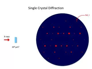
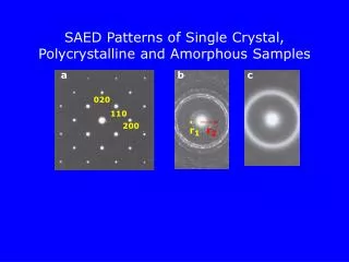
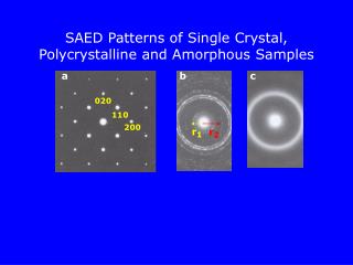
SAED Patterns of Single Crystal, Polycrystalline and Amorphous Samples. a. b. c. 020. 110. 200. r 1. r 2. Geometry for e-diffraction. Electron Diffraction. . Bragg’s Law : l = 2dsin . e -. l =0.037Å (at 100kV) =0.26 o if d=4Å. d hkl. Specimen foil. l = 2d . L 2 .

E N D
SAED Patterns of Single Crystal, Polycrystalline and Amorphous Samples a b c 020 110 200 r1 r2
Geometry for e-diffraction Electron Diffraction Bragg’s Law:l = 2dsin e- l=0.037Å (at 100kV) =0.26o if d=4Å dhkl Specimen foil l = 2d L 2 r/L=sin2 as 0 r/L = 2 r/L = l/d or r = lLx r T D Reciprocal lattice 1 d L -camera length r -distance between T and D spots 1/d -reciprocal of interplanar distance(Å-1) SAED –selected area electron diffraction hkl [hkl] SAED pattern
Ewald’s Sphere Ewald’s sphere is built for interpreting diffraction lkl=1/ Ewald circle C incident beam diffracted beam 2 kd H ki g G 130 0 CG-C0=0G or kd-ki=g Laue equation Wherever a reciprocal lattice point touches the circle, e.g., at G, Bragg's Law is obeyed and a diffracted beam will occur. At H, no diffraction.
Convergent Beam Electron Diffraction (CBED) CBED uses a conver- gent beam of elec- trons to limit area of specimen which con- tributes to diffraction pattern. Each spot in SAED then becomes a disc within which variations in intensity can be seen. CBED patterns contain a wealth of information about symmetry and thickness of specimen. Big advantage of CBED is that the information is generated from small regions beyond reach of other techniques.
SAED vs CBED Parallel beam Convergent beam Spatial resolution >0.5m Spatial resolution beam size Convergence angle sample objective lens spots disks T D T D SAED CBED
CBED-example 2 HOLZ HOLZ - High Order Laue Zone
Applications of CBED • Phase identification • Symmetry determination-point and • space group • Phase fingerprinting • Thickness measurement • Strain and lattice parameter measurement • Structure factor determination
Phase Identification in BaAl2Si2O8 Hexagonal Orthorhombic Hexagonal 6mm 6mm 2mm 800oC 200oC 400oC <0001>
Phase Fingerprinting By CBED Orthorhombic AFE Cubic PE [001] CBED patterns of an antiferroelectric PbZrO3 single crystal specimen at (a) 20oC, (b) 280oC, (c)220oC. (d) [001] CBED pattern of a rhombohedral ferroelectric Pb(ZrTi)O3 Specimen at 20oC. Rhombohedral FE Rhombohedral FE
Symmetry and Lattice Parameter Determination CBED EDS A BF A B 010 Nb A B 001 [100] B SAED 0.2m B A A [111] CBED-HOLZ [143] B Lattice parameters Experimental simulated