Download
1 / 46
460 likes | 547 Vues
Learn about Transition-Edge Sensor (TES) technology being utilized in a large area array for particle-induced X-ray emission spectroscopy. TES acts as a calorimeter, detecting radiation with high energy sensitivity and resolution. Discover the setup, specifications, measurements, and future enhancements of this advanced system.

E N D
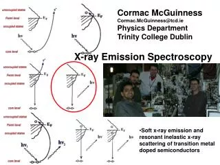
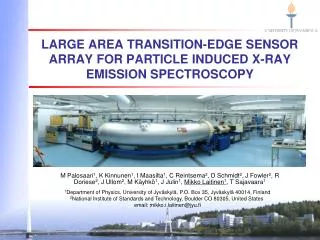
Large area transition-edge sensor array for particle induced X-ray emission spectroscopy M Palosaari1, K Kinnunen1, I Maasilta1, C Reintsema2, D Schmidt2, J Fowler2, R Doriese2, J Ullom2, M Käyhkö1, J Julin1, Mikko Laitinen1, T Sajavaara1 1Department of Physics, University of Jyväskylä, P.O. Box 35, Jyväskylä 40014, Finland 2National Institute of Standards and Technology, Boulder CO 80305, United States email: mikko.i.laitinen@jyu.fi
Transition-Edge Sensor (TES) • TES as a calorimeter • Measures the energy of incident radiation Typical pulse from a calorimeter Schematics of a calorimeter
TES Operation • Operates between superconducting and normal state • Extremely sensitive R(T) • Excellent energy resolution • Wide energy range • Detects radiation,in our case X-rays • Particles also possible Normal state transition edge Superconducting state Typicaltransition of a TES
TES basics • TES thin film device is made of normal metal - superconducting metal bilayer. • The absorber details depend on the desired energy range. • TESs are usually fabricated on thin SiN membranes to limit the thermal conductivity G. In typical TES array, all pixels different -> automated calibration essential Photograph of a 256 pixelTES array made in VTT, Finland.
Details inside the instrument ~15 mm ~300 mm
Jyväskylä TES specifications • 160 pixels from NIST, upgradable to 256 (from VTT) • Total area with 160 pixels ~16 mm2 • Single pixel count rate limited to <20 Hz, typical value 10 Hz • 2 mm thick Bi absorber with Mo/Cu superconducting juction • Detection efficiencieswith 100 um of Be:80 % at 5 keV,20 % at 10 keV, 5 % at 30 keV • Low energies limited byMeV particle absorber,probably not needed
PIXE-TES results from Jyväskylä Roughly one year ago: 12 pixels Mn Kα from Fe-55 source Best pixel Instrumental resolution for the best pixel with 55Fe source was 3.06 eV
PIXE-TES results from Jyväskylä Now: 160 pixels… • But, Computer interface and I/O cards cannot handle all pixels simultaneously • I/O card + PC update coming from NIST to finally secure the function of all 256 possible channels, simultaneously. This month: data with Fe-55 source Resolution around 5 eVfor combined 40 pixels, Improvement seen bybetter data analysis
PIXE-TES results from Jyväskylä SRM-611, trace elements in glass All TES data shown was analyzed last week, 1 eV / bin Analysis resolution for all of these plots ~10 eV
PIXE-TES results from Jyväskylä SRM-611, trace elements in glass
PIXE-TES results from Jyväskylä SRM-611, trace elements in glass Differences between pixels which are not only statistics
PIXE-TES results from Jyväskylä SRM-1157, speciality tool steel No Si escape peak Bi escape peaks Single measurement, wide energy range
PIXE-TES results from Jyväskylä SRM-1157, speciality tool steel V, Cr, Mn, Fe separated
In the NearFuture • Read-out upgraded to full scale. • Modification of PIXE setup to be able to measure samples in atmosphere. • Study art samples in a project that just started • X-ray measurements with our own detector array fabricated by VTT. • Study the satellite peaks with different ions and energies. • ->> Chemical information from wide energy/elemental range ???
Conclusions • Instrumental resolution of 3 eV demonstrated • Combined pixel resolution of ~5 eV looks realistic • Wide energy scale (“0” to tens of keV) • Reasonable count rates available (10 Hz/pixel, 256 pixels) • Active detector area about 16 mm2 • No liquid He needed for ADR cryo cooler • Largish instrument: ~5 cm sample-to-detector • Data handling and analysis: automation necessary • Is the chemical information achievable, after all ?
t 3-8. July, 2016, in Jyväskylä, Finland
Pixel calibration Single pixel shows Si peaks nicely but without good calibration, sum spectrum useless Sample: SRM-611 No/bad calibration regime good calibration
TES-PIXE data calibration Rawpulseheight datawheresamplewaschanged. Sample 1 Sample 2 Eenergyscale SubstratewasSi for bothsamples Measurementtime/duration
TES-PIXE data • Makingselection to single (example) emission line • Beforelinerfit Straightline to guide the eye
TES-PIXE data • Afterlinearfit Si Si Straightline to guide the eye
PIXE Mn vs. 55Fe Mn Kα from Fe55 source same pixel • What is the origin of the hump?
Detectorperformance: PIXE Mn vs. 55Fe source • Instrumental resolution for the best pixel with 55Fe source was 3.06 eV. • For 2 MeV protons and Mn sample resolution was 4.20 eV. M. Palosaari et. al J. Low Temp. DOI 201310.1007/s10909-013-1004-5
PIXE applications • With betterdetectorsonecouldsee thechemicalenvironmentof the sample. Rev. Sci. Instrum. 78, 073105 (2007) J. Hasegawa et. al • Traditional PIXE applications • Archaeology • Geology • Filters in industry • Old paintings
TES vs. SDD • Impurities in the Cu sample resolved better with TES detector
PIXE Mn vs. 55Fe Mn Kα from Fe55 source same pixel • FWHM broadens less than 1eV.
Example: Thin film with high mass element • Atomic layer deposited Ru film on HF cleaned Si • Scattered beam, 35Cl, used for Ru deph profile • Monte Carlo simulations needed for getting reliable values for light impurities at the middle of the film Ru SiO2 Si Poor E resolution Low energy heavy ion ERDA – See posters!
Example: Diamond-like carbon films • 2.3 µm thick diamond-like-carbon film on Si, measured with 9 MeV 35Cl • All isotopes can be determined for light masses • Light elements can be well quantified (N content 0.05±0.02 at.%) Low energy heavy ion ERDA
ALD 8.6 nm Al2O3/Si • Atomic layer deposited Al2O3 film on silicon (Prof. Ritala, U. of Helsinki) • Density of 2.9 g/cm3 and thickness of 8.6 nm determined with XRR (Ritala) • Elemental concentrations in the film bulk as determined with TOF ERDA are O 60±3 at.%, Al 35±2 at.%, H 4±1 at.%. and C 0.5±0.2 at.%
10 nm CNx on silicon • TOF-ERDA results from sputter deposited 10 nm thick CNx hard coating on Si. Measured with 6 MeV 35Cl beam and extreme glancing angle of 3° • A density of 2.0 g/cm3 was used in converting areal densities to nm
Effect of stripper gas pressure • 13.6 MeV 63Cu7+ CaPO (hydroxyapatite)
Gas ionization detector • Thin (~100 nm) SiN window • Electrons for T2 timing signal emitted from the membrane
Future improvements: Gas ionization detector 30 mm TOF-E results from ETH Zürich Incident ion 12 MeV 127I and borosilicate glass target 200 nm thick SiN membrane from Aalto University, Finland, on 100 mm wafer Nucl. Instr. and Meth. B 248 (2006) 155-162
Gas ionization detector to replace Si-energy detector • Why try to fix a well working system? • Greatly improved energy resolution for low energy heavy ions → heavier masses can be resolved • Gas detector is 1D position sensitive by nature → possibility for kinematic correction and therefore larger solid angles possible • Gas detector does not suffer from ion bombardment Recoil ranges in isobutane 8.5 MeV 35Cl 10.2 MeV 79Br Gas ionization detector develoment – See posters!