Advanced PHENIX Silicon Endcap Physics Measurements and Development Overview
160 likes | 273 Vues
This document outlines significant advances in the PHENIX silicon endcap detector, focusing on measurements related to open charm, beauty production, and displaced vertex triggers. It highlights the collaboration with Fermilab on chip design and development, data handling through high-speed optical links, and various engineering progressions for readout systems. The design incorporates mini-strips for effective vertex reconstruction, fulfilling performance specifications through innovative engineering solutions while ensuring high yield and low noise in detector applications.

Advanced PHENIX Silicon Endcap Physics Measurements and Development Overview
E N D
Presentation Transcript
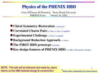
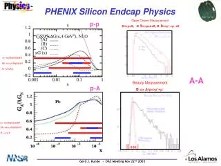
GS95 PHENIX Silicon Endcap Physics Open Charm Measurement D=>m+X, DD=>m+e+X, DD=>m+ +m- +X p-p cc(displaced)X bbe/+displaced BJ/Xg A-A Beauty Measurement B => J/y=>m++m- p-A cc(displaced)X bbe/+displaced BJ/X /100
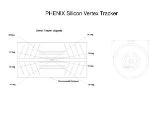
PHENIX Silicon Endcap • Executive Summary • Four umbrella stations on each side matching the large MUON arm acceptace • Mini-strips of 50mu * 2.2 -13 mm (not the BNL detector for S/N reasons) • Readout via new PHX chip from Fermilab (based on existing FNAL chip architecture) • Data push via ~3 Gigabit optical links • Total channel count: 2 Million channels • Total chip count: 4000 chips B -> J/y->m++m-
4608 4096 Preliminary 11/03 Si Umbrella Layout • 50 mu radial pitch (z vertex reconstruction) • 4608 (4096) “mini-strips” • 3.5 cm < r < 18 (14) cm • < 1 % occupancy • 48 “double towers” in phi • mini-strips from 13.0 mm to 2.2 mm • 2 rows of strips per “double tower”, readout via one chip row r = 18.0 cm r = 14.0 cm r = 3.5 cm 1
Collaboration with FNAL • Started to work with Ray Yarema’s group • They did D0 and CDF silicon readout (SVX#) • They developed BTEV prototype (FPIX) • Propose to build PHX, use existing developements … • First simulations for ministrips for PHENIX • Produced preliminary PHX chip layout • Solved readout Endcap bus challenge • Presented at PHENIX Nashville collaboration meeting • Second/Third round of discussions at FEE2003/FNAL • Displaced Vertex Trigger via Data Push • Propose to use FNAL infrastructure to prototype, test and assemble chips and detectors !!!!
FPIX2 Features • Very advanced mixed analog/digital design • Low power (1/10th of ALICE chip) • 128 rows x 22 columns (2816 channels) • 50 µm x 400 µm pixels • High speed readout intended for use in Level 1 trigger. 840 Mbits/sec data output. • Very low noise • Excellent threshold matching • DC coupled input (pixel standart) • Fully programmable device • 3 bit ADC -> basic dE/dx ?
FPIX Measured Performance from Prototype Run FPIX2Threshold Distribution@ Cin= 0 pfis 125 erms FPIX2 noise at C = 0is about 60 erms • Produced ~3000 chips in engineering run • Mixed analog/digital design has excellent performance with insignificant interference and cross talk • Chip size is 8.96 mm x 10.2 mm (91 mm2) • Yield is high • Chip and readout can be used “as is” in other pixel applications [ barrel 1st layer ;-) ] Reminder: MIP in 300 mu Silicon gives 24,000 electrons !!!!
Ray Yarema, FNAL, June 9th Bits and Pieces for Phenix ChipPHX • Use modified FPIX2 front end • Use relaxed bump bonding connections • Use pipeline* and sparsification concepts from SVX4 • Use backside contact for ground return (as done in SVX4) • Use slow programming control from FPIX2 • May use modified output drivers from FPIX2 * possibly data push from FPIX for LV1 trigger purposes
signals & power BUS Bump bonds Programming interface 1st/2nd stage and discriminator Pipeline Digital interface signals & power PHX Chip Layout: 2 columns 256 channels/column 3.8 mm x 13 mm = 49.4 mm2 Bump bonds on 200 um pitch 50 µm dia bumps 512 bumps plus inter-chip bumps for the BUS FPIX2 Layout for comparison: Chip area = 91 mm2 Bump bonds on 50 µm pitch 12 µm dia bumps 2816 bumps
Only “2 ½” Silicon Detector types Outside Detector (IIa) Outside Detector (IIb) Inside Detector (I) 6 chips= 3072 strips 3 chips= 1536 strips Carbon Cooling Wedge 5 chips= 2560 strips
2 silicons in front 2 silicons in back Wedge Assembly Concept 3 mm carbon wedge for assembly and cooling Reason: Eliminate dead silicon areas by overlapping 1 mm along edges ….
Ray Yarema, FNAL, June 9th Proposed PHX R&D Plan • Build first prototype using multiproject submission (40 chips) • Multiple front end designs • Use full sparsification and I/O • Add numerous test points • Chip size = 3.8 mm x 13 mm (full size to understand IR drops and bond to silicon detector) • Fabricate Engineering Run with optimized front end and final digital design (12 wafers) (6000 chips needed) • Started to work with MICRON on test detector (layout of test structure in progress)
Ray Yarema, FNAL, June 9th PHX Development Cost($ Figures requested from FNAL) • Chip design/testing – 2 man-years - $275K (includes all overhead costs) • Prototype chip fabrication- $40K (small chip) • Test board $5K • Engineering run (10-12 wafers) $200K • 5 Extra wafers using same masks - $25K • Production wafer level testing –engineering, tech time, circuit board, probe card - $60K ~ 15 wafers total
Ray Yarema, FNAL, Nov 17th PHX R&D Schedule • Design specifications completed 12/03 • Start design 1/04 • Submit prototype 7/04 • Prototype testing completed 12/04 • Redesign completed for engineering run 1/05 • Engineering run back 3/05 • Endcap proposal to DOE in 12/04
Endcap Summary • Readout and bus via PHX from Fermilab • R&D plan exists • Bump bonded assemblies • Relaxed requirements • Following industry standard • Wedge design • Conceptual design for cooling and assembly • Umbrella endcap • Integration by LANL/Hytec
Si-Umbrellas Si Vertex – Purchased Design Study Conceptual Integration Design by LANL/Hytec (they did Atlas)