Download
1 / 22
230 likes | 462 Vues
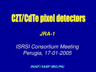
CADMIUM ZINC TELLURIDE (CZT) IMAGER. INTRODUCTION :. SCIENTIFIC REQUIRMENT. 2. DETECTORS USED IN IMAGER. 3. ELECTRICAL CIRCUITS (FRONT END ELECTRONICSUSED) IN THE IMAGER. 4. FUNCTIONING NEW CZT DETECTOR MODULE. 5. DATA ACCUMULATION FROM VARIOUS DETECTOR TO ENCODER.

E N D
CADMIUM ZINC TELLURIDE (CZT) IMAGER INTRODUCTION : • SCIENTIFIC REQUIRMENT 2. DETECTORS USED IN IMAGER 3. ELECTRICAL CIRCUITS (FRONT END ELECTRONICSUSED) IN THE IMAGER 4. FUNCTIONING NEW CZT DETECTOR MODULE 5. DATA ACCUMULATION FROM VARIOUS DETECTOR TO ENCODER 6. GROUNDING SCHEME. 7. COMPONENT LIST USED IN THESE CIRCUITS.
To achieve good spectroscopic capabilities in the range of 10 – 100 KeV • with optimum background counts and spectral resolution, even in • extended energy range up to 1MeV. • Since the detector construction and total area covered is such a way that With help of Coded Aperture Mass (CAM) a moderate image can be studied in 10 -100 KeV energy range. 3)CZT detector (pixilated form) has large energy bandwidth with fine resolution within 10 -100 KeV energy range. 4) Reducing background counts using collimation and anti-coincidence detector (Veto Detector) below the CZT detector plane.
SENSITIVITY OF CZT IMAGER Minimum detectable intensity = 3Nb / (A* T * * E) Photons /(cm2 Sec Sr KeV) Background • WHERE • Nb is background • is detector efficiency δE is the energy interval of observation • T is the integration time flux Source BACKGROUND (Nb) HAS TO BE AS LOW AS POSSIBLE Energy
QUADRANT 4 x 4 MODULE - 500 V XAIM3.2 CHIP CSPA DETECTOR MODULE 16 X 16 CZT PIXEL ARRAY
FUNCTIONAL BLOCK DIAGRAM OF ANLOG CIRCUITS IN XaIm3.2 BIASES USED: 1) Threshold 2) Shaper time 3) Reset width 4) Delay Trigger with help of programming. A
FEATURES OF ASIC XaIm3.2 1.It is fully-driven charge signal acquisition chip. 2.All Analog and Digital outputs are current driven for 1 micro second. Each cell is addressable. 3.Provision of programming for needed parameters of the chip like threshold, shaping time constant and various other parameter. ClkIn and RegIn are Clock and Input for the Shift-resistor. 4.The chip requires +2 and -2 volts for operation. 5.Daisy chaining of chips.
M1 M2 M3 Mn DATA CLOCK ADDR BUS DATA BUS TRIG & MULTI HIT ENERGY PULSE
+V CZT DET OPTO + PROCS ELCTR BF CSPA+ POST AMPLIFIER COMPARATOR AMPL. P.D. + ADC FPGA SCINTILATOR BIAS HV 990V -V HV
15V +5V U13 1 8 9K09 750E NC VCC R53 R55 2 7 R58 Q3 Q4 XAIM_OUTP A B 6K81 3 6 2N2222 2N2222 K C 4 5 47MF Q5 R9 100E K2 E C22 2N2222 Q2 XAIM_OUTM HCPL4562 33E R50 R52 R56 2N2222 1K 460E 1% R51 R49 R54 1K 162E 100E R57 D2 1N4150 14K7 DIFF. AMPLIFIER AMPL.WITH VARIABLE GAIN PEAK DETECTOR ANALOG SWITCH 12-BIT ADC FPGA WINDOW COUNTERS To FPGA SCHEMATIC BLOCK DIAGRAM OF CZT PROCESSING ELECTRONICS
VETO-PMT O/P TO COUNTER AMPTEK 203 POST-AMPL. BIAS VOLTAGE LLD ANALOG SWITCH M_CNTRL PEAK DETECTOR 8-BIT ADC
PRE-AMPL. CsI(Tl) COMPARATOR eV-5128 POST AMPL MONO S 3590 Si PIN PHOTO DIODE BIAS VOLTAGE Schematic block diagram of Alpha –Tag electronics.
F F 1 US M-Rst AD 0 MICRO-CONTROLER PROGRAMMING OF CZT MODULES OPTO LATCH AD 15 1. ANY EVENT MORE THAN LLD THRESHOLDE, TRIGERS THE CZT EVENT ANALYSIS. CZT TRIG. CZT 2. NEXT CZT EVENT WILL ANALYSED ONLY AFTER 12-15 MICRO SEC 12-BIT ADC FPGA VETO 8-BIT ADC 3- LINES OF COUNTERS MULTI-HIT VCO ALPHA-TAG 3-BIT GAIN CNTRL 3-BIT LLD CNTRL VCO CNTRL 3-BIT VETO LLD CNTRL
CZT Trig Pulse (1 U Sec.) CZT WAVEFORMS Processing Time + ADC Conversion Time( 12 U Sec.) CZT Read _Out Pulse (2 U Sec.) Reset Pulse (1 U Sec.) Veto_Trig. Pulse (1 U Sec.) Processing Time +ADC Con. Time (8 U Sec.) VETO WAVEFORMS Read_Out _Time (4 U Sec.) Veto_Reset Pulse
CZT TRIG. PULSE PROCESSING TIME +ADC CONV. TIME READ_OUT TIME RESET VETO TRIG. TIME PROCESSING TIME + ADC CONV. TIME READ_OUT TIME VETO_RESET
LV DC/DC used for powering all detectors and supporting electronics. Conventional High voltage supplies -500 volts for CZT biasing and +1000 volts for Veto PMT. Internal biasing voltages are generated inside the package.
SERIES PASS REGULATOR + V HV POWER OSCI. + RECT.+ MULTI. SECTION CURRENT SENSOR CKT. REFERENCE VOLTAGE CONTRL. Vf DIFFERNTIAL AMPL. Vr COMMANDS
+ 5 V + 10 V O/P Frequency LLD CZT VOLTAGE CONTROL OSCILLATOR LLD VETO MUX 2 kHz TO 20 kHz THERMISTORE HV on-off For Variation of 0-10 volts HV Ref HV Feedback COMMANDS FROM FPGA