Download
1 / 40
400 likes | 556 Vues
This study explores the advantages of 3D micro-structured diamond electrodes for radiation detectors, particularly under ionizing particle exposure. We outline various fabrication techniques, including laser setup and structural characterization, alongside electrical and optical characterization methods. Notably, the 3D geometry enables a higher electric field strength, shorter drift times, and reduced trapping probabilities, leading to improved charge collection efficiency. Our findings underscore the significance of 3D designs in enhancing the performance and reliability of diamond-based radiation detectors.

E N D
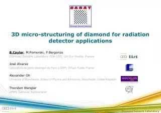
3D micro-structuring of diamond for radiation detector applications • B.Caylar, M.Pomorski, P.Bergonzo • Diamond Sensors Laboratory CEA-LIST, Gif-Sur-Yvette, France • José Alvarez • Laboratoire de génie électrique de Paris (LGEP), Gif-sur-Yvette, France • Alexander Oh • University of Manchester, School of Physics and Astronomy, Manchester, United Kingdom • Thorsten Wengler • CERN, Geneva, Switzerland
Context – Whyusing 3D electrodes? Ionizingparticle Electrodes « Sandwich » 3D Electrodes [1] J.Morse, C.J. Kenney, E.M. Westbrook et al. / Nuclear Instruments and Methods in Physics Research Section A, 524 (2004) 236. • Advantages1: • Higher electric field for a given applied bias voltage • Shorter drift path thus drift time • Lower probability of trapping
Context – Whyusing 3D electrodes? • Planar • 3D • Analyticallycalculatedcurrentsgenerated by a MIP
Context – Whyusing 3D electrodes? • NIEL inducesbulkdefects [2] Michal Pomorski – PhD debate, Frankfurt University 07/08/2008 before irradiation after 1.2 x 10¹⁴ 20MeV n.cm-2 after 1.97 x 10¹⁴ 20MeV n.cm-2 Signal decrease • When flux increases : • Defectsnumberincreases • Carrier lifetime reduction • CCE decreases
Context – Whyusing 3D electrodes? • Planar • 3D • 3D geometry is faster : 8ns vs 208ps. • 3D geometry makes the detector more radiation hard
Outline • Burriedelectrodes • Laser setup & Fabrication • Structural characterization • Electrical characterization • pc-CVD Detector (e6 detector grade) • Electrical characterization • Characterization under alpha particles • sc-CVD Detector (e6 electronic grade) • Optical characterization • Electrical characterization • Transientcurrentmeasurements • Conclusion
Burriedelectrodes – Laser setup 20x Lens Sample holder Nitrogen laser λ = 337nm • τ = 3ns Webcam XYZ Motorized stage • Tunableparameters • Scan velocity 1-1000 µm/s • Laser power 0-160µJ/pulse • Repetition rate 1-30 Hz
Burriedelectrodes – Fabrication Translation Graphitization XYZ Motorized stage • Photoluminescence during • laser processing
Structural characterization – Optical microscopy • Optical grade sc-CVD sample 10µm diameter 20-100 µm diameter 700µm depth 150 µm • Clean surface (Where graphitization starts) • Cracked Surface (Where graphitization ends) • Tilted sample
Structural characterization – 2D Raman mapping • 2D Raman depth mapping obtained by integrating diamond peak 1000 CCD cts 1000 CCD cts Depth 0 CCD cts 0 CCD cts 10µm 10µm • No micro-channel • Micro-channelwith cracks
Structural characterization – SEM imaging H2Plasma • Channel’s clean side after H2 plasma • Channel’s clean side after laser processing
Electrical characterization – I(V) measurements A • ρ(average) = 5.7x10⁻¹ Ω.cm • R(500µm) ~ 2kΩ • Match with nanocrystalline graphite given in literature3 [3] T.Ohana, T.Nakamura, A.Goto et al. / Diamond and Related Materials, 12 (2003) 2011 • Graphite’s channel resitivity
pc-CVD detectorElectrical characterization E6 detector grade 10 x 10 x 0.7 mm3 Sample courtesy Alexander Oh
Electrical characterization – Deviceleakagecurrent A • 3D • Planar • Comparisonbetweenplanar and 3D geometry
Characterization under alpha particles – Experimental setup Fast Charge Sensitive Amplifier M.Ciobanu, GSI, Germany Signal Al back contact FCSA Scope Al front contact Collimator R α Vbias = ±500V Am-241 Source 5.486MeV
Characterization under alpha particles - Results • Planar • 3D • Polarization study – Holes drift (pc-CVD sample)
Characterization under alpha particles - Results • Planar • 3D • Polarization study – Electrons drift (pc-CVD sample)
Characterization under alpha particles - Results α α Amplitude has been normalizedwith the signal of a sc-CVD« e6 electronic grade » diamond • Holes drift (pc-CVD sample)
Characterization under alpha particles - Results α α Amplitude has been normalizedwith the signal of a sc-CVD« e6 electronic grade » diamond • Electrons drift (pc-CVD sample)
Characterization under alpha particles - Analysis α HV +500V V/µm 5 4.5 4 3.5 3 High CCE LowCCE 2.5 700µm 2 1.5 1 200µm 0.5 0 α • Electric field simulation 3D Geometry but pseudo–3D detector
sc-CVD detector E6 electronic grade - <100> oriented 3 x 3 x 0.3 mm3 Sample courtesy Eleni Berdermann
Detector’soptical characterization – Optical microscopy Detector area Test areas • Micro structuredsc-CVDdiamondobservedwithcrossedpolarizers • Bulkstrainmappingafter graphitization
Detector’soptical characterization – Optical microscopy • Detector aftermetallization
Electrical characterization – Deviceleakagecurrent • HV on cracked surface • HV on clean surface • sc-CVD sample after plasma O2 etching
Electrical characterization – Setup and methods • Transientcurrentmeasurements HV +100V 2D Zone 2D Zone 300µm Signal Scope Ultra-Fast 40 dB, 2 GHz Broadband Amplifier Ampli
Transientcurrentmeasurements - Results • Withoutcollimator Mixed e/h drift 1 ns Signal 3D~500mV Electrons drift Signal 2D~80mV Holes drift Signal 2D~100mV • Alphas’ injection on cracked side • Alphas’ injection on clean side
Transientcurrentmeasurements - Results • Withcollimator Mixed e/h drift 1 ns • Alphas’ injection on cracked side
Transientcurrentmeasurements - Analysis • Electric field simulation Planar+3D signal +100 V α V/µm 3 2.5 2 1.5 300µm 1 0.5 0 α Planar signal only
Transientcurrentmeasurements - Results • Experimental results Amplitude ratio = 6 • Selection of relevant events
Transientcurrentmeasurements - Results • Analytically calculated signals Amplitude ratio = 23.8 Amplitude ratio = 22 • Theoriticalresponse • 2GHz lowpassfilter
Transientcurrentmeasurements - Results • Analytically calculated signals • Ampli + devicebandwith~350MHz • Rdevice~ 520Ω • 12channelsconnected • Rchannel ~ 6 kΩ Amplitude’s ratio = 6.2 • 350 MHz lowpassfilter
Conclusion • Conductivegraphitic structures has been achieved on both pc- and sc-CVD sample • These structures are suitable for detectors applications • Twodectetorsusing 3D-geometryelectrodes has been produced • A real improvementbetweenplanar and 3D geometry has ben observed • Higher signal • Fasterresponse • « Polarization effect » decrease on pc-CVD detector • But real 3D detector hasn’t been achievedyet…