Download

1 / 25
250 likes | 350 Vues
Meet the goals of embedding stable channels and finding channel simulants with Lipid Bilayer Ion Channels on a silicon substrate. Address challenges in fabrication through impedance analysis and current-voltage measurements.

E N D
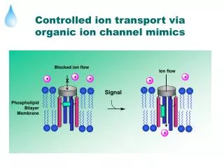
AgCl Electrode Oxide SU-8 Resist Si Project Goals Goal 1:Embed channels in an integrated device that maintains stable potential across them and allows recording of stable, artifact free current through them. Goal 2: Find simulants that bind and transiently block conduction of ions through OmpF.** we shall work with DARPA and other groups within the MOLDICE network to incorporate ion channels that show desired properties Lipid Bilayer with Ion Channels Important building blocks of a fully integrated biosensor with on-chip sensing and signal processing
Technical Approach For the fabrication … Challenges we are facing • silicon substrates are used • layers are structured by • conventional optical lithography • the aperture that supports the • bilayers is constructed using • deep silicon dry etching • relation between the size of the • lipid bilayer and its stability and • the signal-to-noise ratio of the • ion channel response • ultimate limit for the size scaling • of the sensor • optimal surface treatment for • bilayer attachment • stability of the integrated • reversible Ag/AgCl electrodes • manufacturability of the sensor • usability issues (reusability, • cleaning, automation) Experiments involve … • impedance analysis of bilayers • current-voltage measurements • of bilayers and porin channels • studying the influence of surface modification layers on bilayer Gigaseal formation
Summary sheet Milestones Accomplishments • maintain stable potential • (± 1 mV for 1 hour) across a • single channel of OmpF porin • recording of stable, artifact- • free current voltage curves • (± 100 pA for 1 hour) from a • single channel of OmpF porin • using external electrodes • recording stable current • voltage curves using inte- • grated Ag/AgCl electrodes • design and process flow-chart • for a silicon bilayer support chip • working proof-of-concept in form • of a silicon chip as a direct Teflon • membrane replacement • Gigaseal formation proven • channel insertion succeeded • PTFE layers deposited by plasma • CVD facilitate bilayer formation • planar AgCl electrodes exhibit • desired properties
Summary sheet Demonstration of Results Technology Transition • measure sealing resistance • on samples with different • geometries and surface • properties • measure Nernst potential of • Ag/AgCl electrodes • measure DC potential across • porin • measure current through porin • construct a silicon-based sensor • template (reusable if possible) • along with a fixture to allow easy • bilayer formation and protein • insertion • development of a procedure to • reproducibly create bilayers with • Gigaseals • work with DARPA and other • groups within the MOLDICE net- • work to incorporate ion channels • that show desired properties
150 mm 150 mm 825 Resist, 1 mm thickness SU-8 Resist Si Si Si Substrate AZ 4330 Resist, 2.6 mm thickness AgCl Electrode, up to 1 mm thickness Thermally Grown Oxide, d = 500 nm AgCl SU-8 Resist Si Si Si 250 mm 1 mm Hydrophobic Layer 300 mm 150 mm 50 mm SU-8 Resist Photoresist Si AgCl Si SU-8 Resist Si Bilayer Process Flow Resist for Initial Hole Etching Small Hole Etching AgCl Electrode Large Hole Etching Thermal Oxidation Surface Modification Layer Resist for Small Hole Etching SU-8 Resist (Epoxy) Lipid Bilayer Attachment
Process optimization 250 mm • deep silicon etch process that • is optimized on high etch rate • (4.7 mm/min), good selectivity • (220:1) and a concave bottom • profile • etch process that exhibits vertical • sidewalls and a low aspect ratio • dependent etch rate of 3.7 mm/min • with planar bottom profiles below • 100 mm ridge width
Process optimization 250 mm • switch to double-side polished • 100 mm (4”) wafer with 380 mm • thickness allows the fabrication • of multiple samples per run with • identical geometry • front and backside have a smooth • surface and the etching does not • roughen the lower surface • optimized backside alignment re- • sults in good centering of the hole
Sample comparison 250 mm • conventional hole preparation • using electrical discharge to • create an aperture in a PTFE • sheet of 25 mm thickness • using deep silicon dry etching • and back side alignment photo- • lithography a small hole (150 mm) • was created inside a recess
PTFE Surface Modification • the stability of the lipid bilayer • is related to the contact angle • between the bilayer and the • supporting substrate • water contact angle measure- • ments can be used to determine • the substrate’s surface energy Torus g Bilayer Substrate • coating the oxide surface with a • Teflon film changes its properties • from hydrophilic to hydrophobic • (small to large contact angle) • using Plasma CVD is a novel • method that provides an easy • way to deposit thick PTFE layers
Hole diameter = 150 mm PTFE coated surface Lipid Bilayer Experiments • Experiment showing the opening of a single • OmpF porin channel. The vertical lines • through the red current trace are an artifact • from stirring of the bath to facilitate the • insertion of porin into the bilayer membrane. • Plot showing the different levels of OmpF • porin (Trimer). Level 1 is not shown. All the • traces in the above plot are from the same • OmpF porin bilayer experiment using the • silicon wafer coated with PTFE (Teflon).
Lipid Bilayer Experiments • physiological behavior of OmpF • response is indistinguishable • from channels in Teflon • supported membranes • reproducibility of measurements • and voltage dependence • indicates that switching is not an • artifact but real channel activity
Integrated AgCl Electrodes AgCl ring on oxide AgCl ring on SU-8 (chloridized) Schematic view of the electrode layout 3 mm • silver is evaporated on both • sides of the wafer (> 500 nm) • layer patterning by photo- • lithography and etching • chloridization in 5% NaOCl • for 30 sec • measurements are performed • using 0.1M or 0.5M KCl • reference solutions
Integrated AgCl Electrodes AgCl layer, chloridized in 5% NaOCl 10 8 0.5M (trans) and 0.6M (cis) 0 KCl Test solutions 6 -20 4 2 Potential difference (mV) -40 Potential difference (mV) 0 -2 -60 -4 -6 -80 Simulation -8 Measurement -10 -100 0 1 2 3 4 5 0 1 2 3 4 5 Time (h) AgCl Electrode Potential, Single substrate 0.1M KCl Reference solution KCl Molarity difference (M) • minimal difference between the • expected and measured Nernst • potential variation with KCl • concentration • no notable difference between • electrodes on oxide and epoxy • good potential stability of • the microstructured electrodes
AgCl Electrode AgCl layer after 5 h measurement AgCl layer before measurement • difference between expected • and measured potential due to • partially chloridized surface • longterm failure mechanism: • AgCl gets dissolved in the KCl • electrolyte
Theory, Simulation, Experiment show Crowded Charge Selectivity Make a Calcium Channel by Site-directed Mutagenesis George Robillard, Henk Mediema, Wim Meijberg BioMaDe Corporation, Groningen, Netherlands
D113 D113 E117 E117 Site-directed R132 E132 mutagenesis R82 A82 R42 E42 Wild type WT EAE mutant Strategy Use site-directed mutagenesis to put in extraglutamates and create anEEEElocusin the selectivity filter of OmpF George Robillard, Henk Mediema, Wim Meijberg BioMaDe Corporation, Groningen, Netherlands
Ca2+ over Cl- selectivity (PCa/PCl) recorded in 1 : 0.1 M CaCl2 IV-Plot Zero-current potential or reversal potential = measure of ion selectivity Henk Mediema Wim Meijberg
Make a Calcium Channel by constructing the right Charge, Volume, Dielectric Selectivity arises from Electrostatics and Crowding of Charge Precise Arrangement of Atoms is not involved
Conclusions Accomplishments Future work under Phase I • a silicon bilayer support chip has • been constructed and successful • Gigaseal formation has been • demonstrated • channel insertion succeeded • first milestones have been • achieved • integration of the reversible • electrodes demonstrated • PTFE layers deposited by plasma • CVD exhibit excellent properties • measure single channels in an integrated device • study the relation between the size of the lipid bilayer and the signal-to-noise ratio • find optimal surface treatment for bilayer attachment • find simulants that bind and transiently block conduction of ions through ompF • work with DARPA and other groups MOLDICE groups to incorporate ion channels that show desired properties
Si Bilayer 2) Project Goals 1) Project Details Title: Integrated Nanoscale Ion Channel Sensor Start Date: December 15th 2003 End Date: December 31st 2004 (Phase I) Partners: Marco Saraniti (IIT) Bob Eisenberg (Rush) Steve Goodnick (ASU) Trevor Thornton (ASU) • embed channels in a membrane device that maintains stable potential across them and allows recording of stable, artifact free current through them. • Simulants will be found that bind and transiently block conduction of ions through ompF. Plus: Dr. J. Tang (Rush), Dr. M. Goryll (ASU), Dr. G. Laws (ASU), Mr. S. Wilk (ASU) and Mr. D. Marreiro (IIT) 3) “Phase I’ Deliverables 4) Future Plans - issues to be addressed • membrane stabilization • simulants detection • identifying stochastic signatures • ……….. ▪ demonstrate ‘Gigaseal’ properties ▪ demonstrate reversible electrodes ▪ measure single channels with integrated device ▪ characterize stability of integrated device