The silicon substrate and adding to it—Part 1
300 likes | 481 Vues
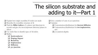
The silicon substrate and adding to it—Part 1. Explain how single crystalline Si wafers are made Describe the crystalline structure of Si Find the Miller indices of a planes and directions in crystals and give the most important direction/planes in silicon

The silicon substrate and adding to it—Part 1
E N D
Presentation Transcript
The silicon substrate and adding to it—Part 1 • Explain how single crystalline Si wafers are made • Describe the crystalline structure of Si • Find the Miller indices of a planes and directions in crystals and give the most important direction/planes in silicon • Use wafer flats to identify types of Si wafers • Define • Semiconductor • Doping/dopant • Resistivity • Implantation • Diffusion • p-n junction • Give a number of uses of p-n junctions • Calculate • Concentration distributions for thermal diffusion • Concentration distributions for ion implantation, and • p-n junction depths
Silicon—The big green Lego® siliconsubstrate siliconsubstrate Surface micromachining Bulk micromachining
Three forms of material Grains Crystalline Amorphous Polycrystalline Glass and fused quartz, polyimide, photoresist Silicon wafers Polysilicon (in surface μ-machining)
Creating silicon wafers • Creates crystalline (cristalino) Si of high purity • A “seed” (semilla) of solid Si is placed in molten Si—called the melt—which is then slowly spun and drawn upwards while cooling it. • Crucible and the “melt” turned in opposite directions • Wafers cut from the cross section. The Czochralski method
Creating silicon wafers Grains Polycrystalline silicon (American Ceramics Society) Photo (foto) of a monocrystalline silicon ingot
It’s a crystal a a a Face-centered cubic (FCC) Body-centered cubic (BCC) Cubic Unit cells a - lattice constant, length of a side of a unit cell
It’s a crystal The diamond (diamante) lattice
Miller indices The Miller indices give us a way to identify different directions and planes in a crystalline structure. • How to find Miller indices: • Identify where the plane of interest intersects the three axes forming the unit cell. Express this in terms of an integer multiple of the lattice constant for the appropriate axis. • Next, take the reciprocal of each quantity. This eliminates infinities. • Finally, multiply the set by the least common denominator. Enclose the set with the appropriate brackets. Negative quantities are usually indicated with an over-score above the number. • Indices: h, k and l • [h k l ] a specific direction in the crystal • <h k l > a family of equivalent directions • (h k l ) a specific plane • {h k l } a family of equivalent planes
Tetoca a ti Find the Miller indices of the plane shown in the figure. • How to find Miller indices: • Identify where the plane of interest intersects the three axes forming the unit cell. Express this in terms of an integer multiple of the lattice constant for the appropriate axis. • Next, take the reciprocal of each quantity. This eliminates infinities. • Finally, multiply the set by the least common denominator. Enclose the set with the appropriate brackets. Negative quantities are usually indicated with an over-score above the number. 4 • Respuesta: (2 4 1) 3 2 1 c b a 1 1 2 2 For cubic crystals the Miller indices represent a direction vector perpendicular to a plane with integer components. Esdecir, [h k l] ⊥ (h k l) ¡Ojo! Not true for non-cubicmaterials!
Non-cubic material example Quartz is an example of an important material with a non-cubic crystalline structure. (http://www.jrkermode.co.uk/quippy/adglass.html)
Miller indices What are the Miller indices of the shaded planes in the figure below? • (1 0 0) • (1 1 0) • (1 1 1) Tetoca a ti: Find the angles between {1 0 0} and {1 1 1} planes, and {1 1 0} and {1 1 1} planes.
Wafer types Si wafers differ based on the orientation of their crystal planes in relation to the surface plane of the wafer. • Wafers “flats” are used to identify • the crystalline orientation of the surface plane, and • whether the wafer is n-type or p-type. <1 0 0> direction (1 0 0) wafer
Relative position of crystalline planes in a (100) wafer Orientations of various crystal directions and planes in a (100) wafer (Adapted from Peeters, 1994)
It’s a semiconductor Conductors Insulators Semiconductors The “jump” is affected by both temperature and light sensors and optical switches
Conductivity, resistivity, and resistance • Electrical conductivity (σ) • A measure of how easily a material conducts electricity • Material property • Electrical resistivity (ρ) • Inverse of conductivity; esdecirρ = 1/σ • Material property By doping, the resistivity of silicon can be varied over a range of about 1×10⁻⁴ to 1×10⁸Ω•m!
Conductivity, resistivity, and resistance • Tetoca a ti • Find the total resistance (in Ω) for the MEMS snake (serpiente) resistor shown in the figure if it is made of • Aluminum (ρ = 2.52×10⁻⁸Ω·m) and • Silicon 1 μm 100 bends total • Respuesta: • Al: 509 Ω • Si: 1.3 GΩ !! 100 μm 1 μm Entire resistor is 0.5 μm thick
Doping Phosphorus is a donor – donates electrons Boron is an acceptor – accepts electrons from Si Charge carriers are “holes.” Phosphorus and boron are both dopants. P creates an n-type semiconductor. B creates a p-type semiconductor.
Doping • Two major methods • Build into wafer itself during silicon growth • Gives a uniform distribution of dopant • Background concentration • Introduce to existing wafer • Implantation or diffusion (or both!) • Non-uniform distribution of dopant • Usually the opposite type of dopant (Esdecir, si wafer es p-type, el otroes n-type y vice versa) • Location where dopant concentration matches background concentration se llama p-n junction p-n junction • Uses of doping and p-n junctions: • Change electrical properties (make more or less conductive) • Create piezoresistance, piezoelectricity, etc. to be used for sensing/actuation • Create an etch stop
Doping How do we determine the distribution of diffused and/or implanted dopant? Mass diffusion: Often implantation and diffusion are done through masksin the wafer surface in order to create p-n junctions at specific locations. Concentration gradient Mass “flux” Diffusion constant Compare to Frequency factor and activation energy for diffusion of dopants in silicon
Doping by diffusion C time x At t = 0, or C(x, t = 0) = 0 Conservation of mass (applied to any point in the wafer) • Need • 1 initial condition • 2 boundary conditions C(x = 0, t > 0) = Cs C(x → ∞, t > 0) = 0 erfc() is the complementary error function: Appendix C Solución
Doping by diffusion x Diffusion length rough estimate of how far dopant has penetrated wafer Diffusion of boron in silicon at 1050°C for various times
Doping by diffusion Total amount of dopant diffused into a surface per unit area is called the ion dose. Cs C(x = 0, t > 0) = Cs Q = constant time Gaussian distribution x
Doping by implantation Distribution is also Gaussian, but it is more complicated. • CP – peak concentration of dopant • RP–the projected range (the depth of peak concentration of dopant in wafer) • ΔRP– standard deviation of the distribution • Range affected by the mass of the dopant, its acceleration energy, and the stopping power of the substrate material. Doping by ion implantation Peak concentration
Doping by implantation Doping is often (de hecho, usually) a two-step process: 1st implantation – pre-deposition 2nd thermal diffusion – drive-in If projected range of pre-deposition is small, can approximate distribution with Typical concentration profiles for ion implantation of various dopant species Replace with Qi
Junction depth C implanted dopant background concentration p-n junction x
Tetoca a ti • A n-type Si-wafer with background doping concentration of 2.00×1015cm-3 is doped by ion implantation with a dose of boron atoms of 1015cm-2, located on the surface of the wafer. Next thermal diffusion is used for the drive-in of boron atoms into the wafer a 900°C for 4 hours. • a. What is the diffusion constant of boron in silicon at this temperature? • b. What is the junction depth after drive-in? • Hints: • Assume that the distribution of ions due to implantation is very close to the wafer surface • Useful information: • kb= 1.381×10⁻²³ J/K • eV = 1.602×10⁻¹⁹ J
Tetoca a ti • A n-type Si-wafer with background doping concentration of 2.00×1015cm-3 is doped by ion implantation with a dose of boron atoms of 1015cm-2, located on the surface of the wafer. Next thermal diffusion is used for the drive-in of boron atoms into the wafer a 900°C for 4 hours. • a. What is the diffusion constant of boron in silicon at this temperature? • b. What is the junction depth after drive-in? Set = Cbg = 1.248×10⁻¹⁸ m2/s b. a. = 0.83×10⁻⁶ m Replace with Qi