Download

1 / 132
1.45k likes | 1.9k Vues
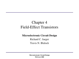
MOS Field-Effect Transistors (MOSFETs). 1. Figure 4.1 Physical structure of the enhancement-type NMOS transistor: (a) perspective view; (b) cross-section. Typically L = 0.1 to 3 m m, W = 0.2 to 100 m m, and the thickness of the oxide layer (t ox ) is in the range of 2 to 50 nm.

E N D
MOS Field-Effect Transistors (MOSFETs) 1
Figure 4.1 Physical structure of the enhancement-type NMOS transistor: (a) perspective view; (b) cross-section. Typically L = 0.1 to 3 mm, W = 0.2 to 100 mm, and the thickness of the oxide layer (tox) is in the range of 2 to 50 nm. Microelectronic Circuits - Fifth Edition Sedra/Smith
Ingat pada p-n junction Figure 4.2 The enhancement-type NMOS transistor with a positive voltage applied to the gate. An n channel is induced at the top of the substrate beneath the gate. Microelectronic Circuits - Fifth Edition Sedra/Smith
Figure 4.3An NMOS transistor with vGS > Vt and with a small vDS applied. The device acts as a resistance whose value is determined by vGS. Specifically, the channel conductance is proportional to vGS – Vt’ and thus iD is proportional to (vGS – Vt) vDS. Note that the depletion region is not shown (for simplicity). Microelectronic Circuits - Fifth Edition Sedra/Smith
Figure 4.4 The iD–vDS characteristics of the MOSFET in Fig. 4.3 when the voltage applied between drain and source, vDS, is kept small. The device operates as a linear resistor whose value is controlled by vGS. Microelectronic Circuits - Fifth Edition Sedra/Smith
Figure 4.5 Operation of the enhancement NMOS transistor as vDS is increased. The induced channel acquires a tapered shape, and its resistance increases as vDS is increased. Here, vGS is kept constant at a value > Vt. Microelectronic Circuits - Fifth Edition Sedra/Smith
Figure 4.6 The drain current iD versus the drain-to-source voltage vDS for an enhancement-type NMOS transistor operated with vGS > Vt. Microelectronic Circuits - Fifth Edition Sedra/Smith
Figure 4.7 Increasing vDS causes the channel to acquire a tapered shape. Eventually, as vDS reaches vGS – Vt’ the channel is pinched off at the drain end. Increasing vDS above vGS – Vt has little effect (theoretically, no effect) on the channel’s shape. Microelectronic Circuits - Fifth Edition Sedra/Smith
Equipotential pada arah y (melebar) Kapasitansi gate-channel (dielektrik SiO2) per satuan area (1) (2) Muatan tersimpan dalam Kapasitor (3) Muatan tersimpan dalam “potongan” equipotensial (4) Figure 4.8 Derivation of the iD–vDS characteristic of the NMOS transistor. Microelectronic Circuits - Fifth Edition Sedra/Smith
sehingga Muatan pada celah potongan Medan listrik pada “potongan” Laju elektron (drift) Karena medan listrik Arus drift pada celah “potongan” Figure 4.8 Derivation of the iD–vDS characteristic of the NMOS transistor. Microelectronic Circuits - Fifth Edition Sedra/Smith
Arus drain yang disebabkan arus drift pada celah “potongan” dapat disusun menjadi Integrasi dengan batas source dan drain atau x antar 0 dan L dan tegangan 0 dan vDS memberikan arus drain menjadi Untuk saturasi Microelectronic Circuits - Fifth Edition Sedra/Smith
definisi konstanta Microelectronic Circuits - Fifth Edition Sedra/Smith
Figure 4.9 Cross-section of a CMOS integrated circuit. Note that the PMOS transistor is formed in a separate n-type region, known as an n well. Another arrangement is also possible in which an n-type body is used and the n device is formed in a p well. Not shown are the connections made to the p-type body and to the n well; the latter functions as the body terminal for the p-channel device. Microelectronic Circuits - Fifth Edition Sedra/Smith
Potongan melintang Layout Microelectronic Circuits - Fifth Edition Sedra/Smith
Perhatikan: arah panah menunjukkan arah junction seperti pada dioda Kanal tipe n dan bodi tipe p Figure 4.10 (a) Circuit symbol for the n-channel enhancement-type MOSFET. (b) Modified circuit symbol with an arrowhead on the source terminal to distinguish it from the drain and to indicate device polarity (i.e., n channel). (c) Simplified circuit symbol to be used when the source is connected to the body or when the effect of the body on device operation is unimportant. Microelectronic Circuits - Fifth Edition Sedra/Smith
Perilaku arus-tegangan MOSFET dan Daerah Operasinya Pengukuran/ Karakterisasi Figure 4.11 (a) An n-channel enhancement-type MOSFET with vGS and vDS applied and with the normal directions of current flow indicated. (b) The iD–vDS characteristics for a device with k’n(W/L) = 1.0 mA/V2. Microelectronic Circuits - Fifth Edition Sedra/Smith
Daerah Trioda Syarat 1. kanal terbentuk 2. Kanal kontinyu “Bentuk” Kanal Kanal kontinyu atau tegangan gate-drain masih membentuk kanal (daerah deplesi belum terlalu besar sehingga membuat kanal Pinch-off) Persamaan arus-tegangan atau Microelectronic Circuits - Fifth Edition Sedra/Smith
Daerah Trioda Persamaan arus-tegangan untuk menjadi dapat dinyatakan sebagai Dengan definisi menjadi Mengapa DS huruf kapital? syarat Microelectronic Circuits - Fifth Edition Sedra/Smith
Daerah Saturasi Syarat 1. kanal terbentuk 2. Pinch-off “Bentuk” Kanal Kanal pinch-off, tegangan gate-drain tidak lagi membentuk kanal, arus drain hanya ditentukan jumlah muatan yang dibentuk tegangan gate pada kanal Persamaan arus-tegangan atau Microelectronic Circuits - Fifth Edition Sedra/Smith
Daerah Saturasi Persamaan arus-tegangan Untuk drain-gate terhubung singkat MOSFET selalu saturasi karena Figure 4.12 The iD–vGS characteristic for an enhancement-type NMOS transistor in saturation (Vt = 1 V, k’nW/L = 1.0 mA/V2). Microelectronic Circuits - Fifth Edition Sedra/Smith
Figure 4.13 Large-signal equivalent-circuit model of an n-channel MOSFET operating in the saturation region. Microelectronic Circuits - Fifth Edition Sedra/Smith
Figure 4.14 The relative levels of the terminal voltages of the enhancement NMOS transistor for operation in the triode region and in the saturation region. Microelectronic Circuits - Fifth Edition Sedra/Smith
Setelah mencapai saturasi apabila tegangan drain-source masih dinaikkan, maka panjang kanal berkurang Persamaan arus semula menjadi disusun ulang untuk dapat didekati dengan sebanding dengan sehingga dan dapat dinyatakan dengan Figure 4.15 Increasing vDS beyond vDSsat causes the channel pinch-off point to move slightly away from the drain, thus reducing the effective channel length (by DL). Microelectronic Circuits - Fifth Edition Sedra/Smith
untuk maka ID Definisikan maka sehingga atau dimana Figure 4.16 Effect of vDS on iD in the saturation region. The MOSFET parameter VA depends on the process technology and, for a given process, is proportional to the channel length L. Microelectronic Circuits - Fifth Edition Sedra/Smith
Figure 4.17 Large-signal equivalent circuit model of the n-channel MOSFET in saturation, incorporating the output resistance ro. The output resistance models the linear dependence of iD on vDSand is given by Eq. (4.22). Microelectronic Circuits - Fifth Edition Sedra/Smith
Daerah Trioda Syarat 1. kanal terbentuk 2. Kanal kontinyu Persamaan arus-tegangan dengan Daerah Saturasi Syarat 1. kanal terbentuk 2. Pinch-off Persamaan arus-tegangan Figure 4.18(a) Circuit symbol for the p-channel enhancement-type MOSFET. (b) Modified symbol with an arrowhead on the source lead. (c) Simplified circuit symbol for the case where the source is connected to the body. (d) The MOSFET with voltages applied and the directions of current flow indicated. Note that vGS and vDS are negative and iD flows out of the drain terminal. Microelectronic Circuits - Fifth Edition Sedra/Smith
Figure 4.19 The relative levels of the terminal voltages of the enhancement-type PMOS transistor for operation in the triode region and in the saturation region. Microelectronic Circuits - Fifth Edition Sedra/Smith
Vt=-1V, kp’=60mA/V2, W/L=10, hitung • VG agar FET konduksi • VD untuk triode • VD untuk saturasi • untuk l=0, |VOV|, VG dan VD untuk ID=75mA • ro untuk l=-0,02V-1 dan |VOV| dari (d) • ID untuk l=-0,02V-1 dan |VOV| dari (d) pada VD=+3V dan VD=0V, lalu hitung ro dan bandingkan dengan (e) (a) Syarat (b) Syarat (c) Syarat Figure E4.8 Microelectronic Circuits - Fifth Edition Sedra/Smith
(d) Asumsi saturasi (e) (f) Untuk ini sama! Figure E4.8 Microelectronic Circuits - Fifth Edition Sedra/Smith
Table 4.1 Microelectronic Circuits - Fifth Edition Sedra/Smith
Body Effect pada tegangan threshold Microelectronic Circuits - Fifth Edition Sedra/Smith
ID diinginkan 400mA, VD =0,5V, RD dan RS? Vt=0,7V, mnCox=100mA/V2, L=1mm, dan W=32mm Langkah: 1. Cek konduksi? Cek saturasi atau triode? 2. Hitung VOV 3. Hitung VGS 4. Hitung VS Figure 4.20 Circuit for Example 4.2. Microelectronic Circuits - Fifth Edition Sedra/Smith
ID diinginkan 80mA, R? Vt=0,6V, mnCox=200mA/V2, L=0,8mm, dan W=4mm MOSFET dalam keadaan saturasi (mengapa?) Figure 4.21 Circuit for Example 4.3. Microelectronic Circuits - Fifth Edition Sedra/Smith
Rangkaian pada cabang kanan idem rangkaian sebelumnya, berapa arus pada R=20kW? Berapa tegangan drain? FET Q2 dan Q1 identik Anggap saturasi, VOV pada kedua rangkaian sama, maka arus sama, yaitu 80mA Tegangan VDS=VD>VOV maka FET Q2 dalam keadaan saturasi (anggapan benar) Figure E4.12 Microelectronic Circuits - Fifth Edition Sedra/Smith
Rancang agar VD = 0,1V (atau RD?) Vt=1V, kn’W/L=1mA/V2 FET dalam keadaan trioda, karena sehingga Mengikuti nilai resistor baku yang tersedia untuk Toleransi 5% dapat digunakan 12kW Figure 4.22 Circuit for Example 4.4. Microelectronic Circuits - Fifth Edition Sedra/Smith
Figure 4.23(a) Circuit for Example 4.5. (b) The circuit with some of the analysis details shown. Microelectronic Circuits - Fifth Edition Sedra/Smith
Figure 4.24 Circuit for Example 4.6. Microelectronic Circuits - Fifth Edition Sedra/Smith
Figure 4.25 Circuits for Example 4.7. Microelectronic Circuits - Fifth Edition Sedra/Smith
Figure E4.16 Microelectronic Circuits - Fifth Edition Sedra/Smith
Fungsi R? Figure 4.26(a) Basic structure of the common-source amplifier. (b) Graphical construction to determine the transfer characteristic of the amplifier in (a). Microelectronic Circuits - Fifth Edition Sedra/Smith
Figure 4.26(Continued)(c) Transfer characteristic showing operation as an amplifier biased at point Q. Microelectronic Circuits - Fifth Edition Sedra/Smith
Figure 4.27 Two load lines and corresponding bias points. Bias point Q1 does not leave sufficient room for positive signal swing at the drain (too close to VDD). Bias point Q2 is too close to the boundary of the triode region and might not allow for sufficient negative signal swing. Microelectronic Circuits - Fifth Edition Sedra/Smith
MOSFET saturasi Microelectronic Circuits - Fifth Edition Sedra/Smith
MOSFET triode atau dengan untuk maka Microelectronic Circuits - Fifth Edition Sedra/Smith
Contoh Numerik RD=18kW Vt=1V kn’(W/L)=1mA/V2 VDD=10V Letak X Letak A Letak B Letak C Microelectronic Circuits - Fifth Edition Sedra/Smith
Contoh Numerik 10V Letak Q Q dapat dipilih tepat diantara jangkauan tegangan output atau 5,5V namun untuk mendapat gain yang lebih besar dipilih pada tegangan output 4V 5,5V 4V 2V Microelectronic Circuits - Fifth Edition Sedra/Smith
Contoh Numerik Tegangan input Figure 4.28 Example 4.8. Microelectronic Circuits - Fifth Edition Sedra/Smith
Figure 4.28(Continued) Microelectronic Circuits - Fifth Edition Sedra/Smith
Contoh dengan SPICE Rangkaian Amplifier Sederhana dengan MOSFET Example 4.8 * * Rangkaiannya * * FETnya FET drain gate source body nama_model * M1 out in 0 0 NMOS1 L=1u W=1u * * Resistor drain RD=18k * R1 vdd out 18k * * Power Supply VDD=10V * VDD vdd 0 10 * * Tegangan Input Sinusoidal DC 1.816V Amplitude AC 77mV Frekuensi 10KHz * Alternatif untuk sinyal seperti dalam teks menggunakan PWL * *VS in 0 SIN(1.816 0.075 10k 0 0) VS in 0 PWL(0 1.816 50us 1.741 150us 1.891 250us 1.741 350us 1.891 450us 1.741 500us 1.816) * .MODEL NMOS1 NMOS KP=1e-3 VTO=1 .end .control tran 5us 0.5ms plot in out plot out vs in .end Microelectronic Circuits - Fifth Edition Sedra/Smith
Contoh dengan SPICE Microelectronic Circuits - Fifth Edition Sedra/Smith