Field Effect Transistors (1)
Field Effect Transistors (1). Dr. Wojciech Jadwisienczak. EE314. http://www.plasticlogic.com. Q: How we can do this? A: A new generation of MOSFETs for plastic electronics. Construction of MOS NMOS and PMOS Types of MOS MOSFET Basic Operation Characteristics

Field Effect Transistors (1)
E N D
Presentation Transcript
Field Effect Transistors (1) Dr. Wojciech Jadwisienczak EE314
http://www.plasticlogic.com Q: How we can do this? A: A new generation of MOSFETs for plastic electronics
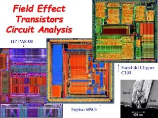
Construction of MOS • NMOS and PMOS • Types of MOS • MOSFET Basic Operation • Characteristics • Small-Signal Equivalent Circuits • Examples Chapter 12: Field Effect Transistors pp. 544-577
Figure 4 – showing the lateral etching control offered by “digital” recess etching. In both micrographs, the depth of the recess is 30 nm. The micrograph on the left shows a “wide” gate recess with large lateral extent whilst the micrograph on the right shows a recess tightly defined around the gate footprint. Figure 2 -120 nm footprint T-gate with self-aligned source and drain contacts. http://www.three-fives.com/latest_features/webzine_features/iainthainestory.html
Building A MOSFET Transistor Using Silicon http://micro.magnet.fsu.edu/electromag/java/transistor/index.html
JFET and MOSFET Transistorsor JFET – Junction Field Effect Transistor MOSFET - Metal Oxide Semiconductor Field Effect Transistor n-channel MOSFET & p-channel MOSFET Symbol L=0.1-10mm W=0.5-500mm SiO2 Thickness=0.05-0.1mm Device characteristics depend on L,W, Thickness, doping levels
n-channel MOSFET Basic Operation Operation in the Cutoff region pn junction: forward bias, reverse bias iD=0 for vGS<Vt0 Schematic When vGS=0 then iD=0 until vGS>Vt0 (Vt0 –threshold voltage)
n-channel MOSFET Basic Operation Operation in the Triode Region For viDS<vGS-Vt0 and vGS>Vt0 the NMOS is operating in the triode region Resistor like characteristic (R between S & D, Used as voltage controlled R) For small vDS, iD is proportional to the excess voltagevGS-Vt0
n-channel MOSFET Basic Operation Operation in the Saturation Region (vDS is increased) Tapering of the channel iD is smaller when vDS is larger When vGD=Vt0 then the channel thickness is 0 and Device parameter KP for NMOSFET is 50 mA/V2
n-channel MOSFET Basic Operation Characteristic Example 12.1 Channel length modulation id depends on vDS in saturation region (approx: iD =const in saturation region)
p-channel MOSFET Basic Operation It is constructed by interchanging the n and p regions of n-channel MOSFET. Symbol Characteristic How does operate p-channel MOSFET? -voltage polarities -iD current -schematic
Load-Line Analysis of NMOS Amplifier It is a graphical analysis similar to load-line analysis of pn diode. Schematic We look for operating point vGS Analysis… vDS Input loop Output loop Load line
Load-Line Analysis of NMOS Amplifier Taking iD=0 or vDS=0 we find out the quiescent operating point Q Load line The quiescent values vin(t)=0 then iDQ=9 mA and vDSQ=11V Points A & B intersection of curve and the load-line
Load-Line Analysis of NMOS Amplifier (peak-to-peak amplitude is 2V) Input signal 12V Inverse operation The positive peak of the input occurs at the same time as the min. value of vDS. These are not symmetrical sinusoids! (nonlinear distortion)
Bias Circuits Analysis of amplifier circuits is often undertaken in two steps: (1) The dc circuit analysis to determine the Q point. It involves the nonlinear equation or the load-line method. This is called bias analysis (2) Use a linear small-signal equivalent circuit to determine circuit parameters The fixed-plus self-bias circuit Equivalent circuit Analysis… vDS vGS Assume the VRG=0 For saturation region Input Output
Bias Circuits Plot of and Disregarded root for vGS<Vt0 Use only larger root for vGS and smaller for iD Example 12.2