Field Effect Transistors in Electronics
Dive into the world of Field Effect Transistors (FETs) and explore their operation, characteristics, biasing methods, and amplification capabilities. Learn about JFETs, MOSFETs, operational amplifiers, and more in this comprehensive e-course module.

Field Effect Transistors in Electronics
E N D
Presentation Transcript
Field Effect Transistors Session 6a for Electronics and TelecommunicationsA Fairfield University E-CoursePowered by LearnLinc Electronics and Telecommunications
Module: Semiconductor Electronics(in two parts) • Text: “Electronics,” Harry Kybett, Wiley, 1986, ISBN 0-471-00916-4 • References: • Electronics Tutorial (Thanks to Alex Pounds) • Electronics Tutorial (Thanks to Mark Sokos) • 5 - Semiconductors, Diodes and Bipolar Transistors • 5 on-line sessions plus one lab • 6 - FETs, SCRs, Other Devices and Amplifiers • 5 on-line sessions plus one lab • Mastery Test part 3 follows this Module Electronics and Telecommunications
Section 6: FETs, SCRs, Other Devices and Operational Amplifiers • 0BJECTIVES:This section reviews additional important semiconductor devices and their applications. The Operational Amplifier is also studied. Electronics and Telecommunications
Section 6 Schedule: Electronics and Telecommunications
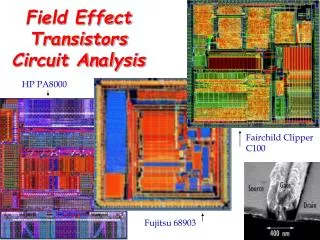
The Field Effect Transistor (FET) • Bipolar Transistor: two diodes, thin base, a current controlled device • FET: A thin current carrying “channel” pinched off by an electric field Electronics and Telecommunications
Junction FET (JFET) • Formed by two diodes back to back • The diodes MUST be reverse biased(forward biasing = high current = poof) • Channel • The current “channel” (drain to source) is lateral through the central material • N-channel - N-type central material • P-channel - P-type central material • Depletion regions (two) pinch off the channel as the diode reverse bias (gate voltage) is increased Electronics and Telecommunications
Junction Diode Operation • PN junction forms at the PN boundary • Holes (P) and free electrons (N) combine • “Depletion” Region forms(no free carriers) • Forward “bias”; allows current • positive voltage on P • negative voltage on N • Reverse “bias”; no current • positive voltage on N • negative voltage on P Electronics and Telecommunications
Insulated Gate FET(MOSFET) • Thin channel isolated from substrate by reverse biased junction • Silicon dioxide insulating layer on top • Metal “Gate” above SiO2 • Capacitor formed between gate and channel • Negative charge on gate (N-channel) repels carriers and pinches off the channel Electronics and Telecommunications
FET Operation • The “Channel” is a conducting path from the source to the drain. • A negative voltage on the “Gate” (for an N-Channel FET) produces an electric field that narrows the channel. • As the gate voltage is made more negative, the gat narrows further thereby increasing the resistance to current flow. • At a still more negative gate voltage the channel is pinched off and no current can flow. • The FET is effectively a voltage controlled resistance Electronics and Telecommunications
Measuring FET Characteristics • Use a potentiometer to vary the gate voltage • Apply a supply voltage from Drain to Source • Measure the drain current Electronics and Telecommunications
FET Characteristic curve • A large negative gate voltage pinches off the channel • As the gate voltage is made less negative, the channel opens and current flows from source to drain until the channel is fully open at about Vg = 0. Electronics and Telecommunications
FET Biasing • The drain/source current raises the average channel voltage • The effective gate voltage is then negative. • A stable or “quiescent” state is achieved. Electronics and Telecommunications
An FET Amplifier Electronics and Telecommunications
Analysis • The gate voltage is zero • DC drain current flows through the source resistor raising the channel voltage till the current stabilizes • An AC signal is superimposed on the gate • The drain current now varies proportionally with the gate voltage causing the drain voltage to also vary. • The AC components of the drain voltage passes through the coupling capacitor to the load resistor. Electronics and Telecommunications
FET Summary • A voltage-controlled resistor • Channel material • N-channel FET • P-channel FET • FET types • Junction FET (JFET) • Metal Oxide Gate FET (MOSFET) • Complementary Symmetry MOSFET (CMOS) • Simple high input impedance amplifiers • Very effective as switches (Session 6b) Electronics and Telecommunications
FET Comparison to Bipolar(Amplifier) Electronics and Telecommunications
Section 6 Schedule: Electronics and Telecommunications