Download
1 / 8
80 likes | 147 Vues
Automated wafer handling has reduced throughput time and increased the efficiency and yield of wafer cassette mapping. To know more, check out the short presentation.

E N D
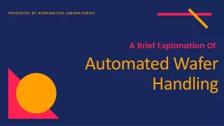
PRESENTED BY KENSINGTON LABORATORIES A Brief Explanation Of Automated Wafer Handling
Nowadays, semiconductor manufacturing industries are fully automated with high-tech environments for handling everything with precision.
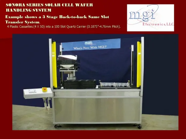
Automated wafer handling has reduced throughput time and increased the efficiency and yield of wafer cassette mapping. The transfer between different processing steps is carried out using FOUPS (front opening unified pods) or special cassettes.
The higher production volume and throughput are essential in the wafer front end. Even if there is a risk of breaking wafers during the transfer, the automated process lessens the chances of any incident.
Wafer Mapping Sensors • The wafer mapping sensors are quick and reliable for detecting the semiconductor wafers. • It is widely used for finding the slotting errors in FOUPs or cassettes. • These sensors are good for detecting the sensitivity of thin and dark-coated wafers of any size. • It can also detect the mixed wafers like Silicon and glass wafers for wafer cassette mapping.
Moreover, the wafer mapping sensors are electrostatic malfunction free with easy maintenance.
TWITTER LINKEDIN YOUTUBE Follow Us On Social Media https://twitter.com/kensingtonlabss https://www.linkedin.com/company/kensington-laboratories https://www.youtube.com/channel%2FUCMvbCR6ni0KAZYnlkUU6Mng
WEBSITE www.kensingtonlabs.com Contact Details PHONE FOR INQUIRIES AND CONCERNS 510.324.0126 FAX EMAIL 510.324.0130 sales@kensingtonlabs.com ADDRESS Kensington Laboratories, LLC 6200 Village Parkway Dublin , CA 94568