Digital Electronics
Digital Electronics. Logic Gates Adders Flip-Flops Registers. Numbers in a computer:. In the Microprocessor and memory Bits are stored electronically Each bit is represented by an electrical signal which is either a high or low voltage level. High 1 and low 0

Digital Electronics
E N D
Presentation Transcript
Digital Electronics Logic Gates Adders Flip-Flops Registers Mark Neil - Microprocessor Course
Numbers in a computer: • In the Microprocessor and memory Bits are stored electronically • Each bit is represented by an electrical signal which is either a high or low voltage level. • High 1 and low 0 • High 0 and low 1 Normal Logic Inverse Logic Mark Neil - Microprocessor Course
CMOS Transistor Transistor Logic (TTL) 3.5 – 4.9 Volts NO MAN’S LAND 74HCxx 2.0 – 2.4 Volts NO MAN’S LAND 74LSxx 0.1 – 1.0 Volts 0.8 – 0.4 Volts High and Low 1:‘High’ 0:‘Low’ It is actually a bit more complicated than this since there are different thresholds for inputs and outputs and their noise margins (indicated here in RED).. Mark Neil - Microprocessor Course
Making a Zero or a One How do you actually make a 0 or 1 ? Pull-up resistor It is clear that depending upon the position of the J1 switch the line will be either ‘0’ or ‘1’ Mark Neil - Microprocessor Course
Making a Zero or a One How do you actually make a 0 or 1 in CMOS? +V +V +V +V BANG! J2 1 0 ? ? J1 “Tri-state” output High impedance Mark Neil - Microprocessor Course
Binary Logic Once the bits are generated, we want to be able to perform various operations on those bits The operations which the microprocessor carries out can all be constructed with a few simple circuits The basic building blocks are logic “gates” Mark Neil - Microprocessor Course
Binary Logic truth tables • You may remember from the first year lab the gates AND, OR, NOT • Any digital device can be made out of either ORs and NOTs or ANDs and NOTs. Mark Neil - Microprocessor Course
DeMorgan’s Theorem You can swap ANDs with ORs if at the same time you invert all inputs and outputs : Exercise: Write truth table for both and prove that this is correct Mark Neil - Microprocessor Course
An AND out of NOTs and ORs Exercise: Test the claim that you can make any logic device exclusively out of NOTs and ORs by making an AND out of NOTs and ORs: Mark Neil - Microprocessor Course
Answer: Show that this device has an identical truth table as the AND gate. Mark Neil - Microprocessor Course
Exercise: Exclusive OR Construct an exclusive OR (XOR) gate using OR, ANDs, and NOT: Mark Neil - Microprocessor Course
The Exclusive OR Solution: Mark Neil - Microprocessor Course
Addition with Binary Logic Gates Computers carry out addition with binary addition of bits stored in registers We can build additions of large numbers of bits out of units which add two bits Example: Adding two 4 bit numbers results in a 4 bit number plus one carry bit or effectively a 5 bit number Lets construct this adder from gates J. Nash - Microprocessor Course
Additions of two bits: The half adder • Adding two bits generates two bits of output • 1 “Sum Bit” S • 1 “Carry Bit” C • The truth table for this operation is shown along with an implementation using two gates Mark Neil - Microprocessor Course
Full Adder • In order to add larger numbers, we need to be able to bring the carry from the lower order bits, and add this to the sum • The inputs are: • the two bits to be added (A,B) • The Carry Bit (C) • The outputs are: • The Sum Bit (S) • The Carry Out Bit (C+) • We can build this from two half adders and an XOR gate Mark Neil - Microprocessor Course
Two bit adder Exercise: Drawa circuit that adds two two bit words (Ao,A1) and (B0,B1) and produces three Sum Bits (S0,S1,S2) We can construct logic that adds more than 1 bit together by using multiple full adder circuits Mark Neil - Microprocessor Course
Solution With the Full adder building block we can generalize to produce a circuit which adds larger numbers Mark Neil - Microprocessor Course
Four plus Four bit addition This can clearly be generalized to any number of bits There is a problem in building circuits this way as the carry bits need to propogate through the circuit before the answer is correct There are other ways to construct adder circuits which avoid this problem Mark Neil - Microprocessor Course
Storing Zeros and Ones: Registers • Registers are electronic devices • capable of storing 0’s or 1’s • D-FLIP-FLOPs are the most elementary registers • can store one bit • 8 DFFs clocked together make a one byteregister • Capable of storing 8 bits Mark Neil - Microprocessor Course
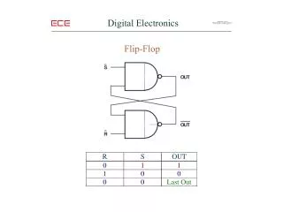
SR Latch: Set and Reset Gate level design of an SR latch • When S* is low and R* High, Q is high (Set) • When S* is high and R* is low Q is cleared (Reset) • Q and Q* are complements Mark Neil - Microprocessor Course
SR Latch: Hold Gate level design of an SR latch • When S* and R* are high both states for Q are possible (and stable) • The latch remembers the last state it was in, and holds Q in that state Mark Neil - Microprocessor Course
SR Latch: Don’t do this… Gate level design of an SR latch • When S* and R* are low Q and Q* are no longer complementary • The latch can also enter a race condition if you try to take S* and R* high again “at the same time” Mark Neil - Microprocessor Course
SR Latch: 1 bit memory Gate level design of an SR latch Ambiguous but stable • S/R high is ambiguous, but stable • This circuit “remembers” that S went low Mark Neil - Microprocessor Course
Gated D Latch Ensures that S and R are always complementary. When the Clock is high – D is set on the outputs of the latch and it is held there when the clock is low Exercise: Fill out the truth table for this circuit. Mark Neil - Microprocessor Course
D latch timing The input Data to the gated D latch appears on the output (Q)while the clock is high. Sometimes we want to transfer the data into the register only at a specified moment (for example when the clock changes) The Master-Slave D Flip-Flop uses two d-latches to latch the data on the edge (depending on the design either positive or negative) of the input clock Mark Neil - Microprocessor Course
Master Slave – D Flip Flop • Data is stored in the “Master” latch (Qm) when the clock is high • When the clock goes from high to low • The data is held in the Master • The Data is stored in the slave latch output • The Qs output can only change when the clock goes from high to low Mark Neil - Microprocessor Course
A real D-Flip-Flop (DFF) One can Set or Reset (Clear) the DFF using S or R When S and R are High, on the rising edge of the clock the data are transferred and stored in Q. Mark Neil - Microprocessor Course
4-bit Register A register that stores 4 bits Data Stored on rising edge of clock in Q0,Q1,Q2,Q3 Datacoming in D0,D1,D2,D3 Mark Neil - Microprocessor Course
Byte Register 8 bit register in a single package 74F574 Also contains tri-state outputs Byte coming in CLK Byte Stored Mark Neil - Microprocessor Course
Arithmetic Logic Unit (ALU) • Centre of every computer • Composed of building blocks we have been learning about • Adders • Flip Flops • Registers • We also need to have a data bus to move data in and out - we will learn about this soon Mark Neil - Microprocessor Course
Exercise: build an external 1 Byte memory * = INVERTED Output Enable* (Read Data) Byte coming in (PORTA) Byte Stored (PORTE) CP (Write Data) Control lines (PORTD) Mark Neil - Microprocessor Course
The data sheets of the 74F574 Mark Neil - Microprocessor Course
The 74F574 outputs The outputs of the 574 are tri-state : They Can be high ‘1’, low ‘0’, and DISCONNECTED (HIGH IMPEDANCE STATE). Mark Neil - Microprocessor Course
The 74F574 Function Table When Output Enable (OE*) is low, the data can be read from the register Data can be written to the register at any time by driving the Clock Pulse (CP) from low to high Mark Neil - Microprocessor Course
Timing diagram: Load Register – Enable Output ts CP D0-D7 tPZH OE O0-O7 ts= setup time tPZH= Output Enable time Mark Neil - Microprocessor Course
Timing diagram: write with OE Low CP D0-D7 (in) OE O0-O7 (out) tp Tp= propagation delay Mark Neil - Microprocessor Course