Download
1 / 15
160 likes | 295 Vues
Analytical 2D Modeling of Sub-100 nm MOSFETs Using Conformal Mapping Techniques. Benjamin Iñiguez Universitat Rovira i Virgili (URV), Tarragona, E-43001, SPAIN, E-mail:binyigue@etse.urv.es Jarle Østhaug, Tor A. Fjeldly UniK- University Graduate Center, N-2027 Kjeller,

E N D
Analytical 2D Modeling of Sub-100 nm MOSFETs Using Conformal Mapping Techniques Benjamin Iñiguez Universitat Rovira i Virgili (URV), Tarragona, E-43001, SPAIN, E-mail:binyigue@etse.urv.es Jarle Østhaug, Tor A. Fjeldly UniK- University Graduate Center, N-2027 Kjeller, NORWAY, E-mail: torfj@unik.no
Need of new compact MOSFET modeling concepts • The behavior of sub-100 nm MOSFETs is critically determined by physical mechanisms that are not observed in larger devices. • To allow circuit designers to use the potentials of sub-100 nm technology, these mechanisms must be formulated and implemented into CAD tools.
Need of a 2-D compact model • The present MOSFET standard models are based on a 1D theory, initially developed for long-channel devices. • Short channel effects have been progressively included (as the feature size has been shrunk down) using additional equations (often empirical). • This has resulted in an enormous increase of the number of parameters.
Purpose of our compact modeling work • We present a new modeling approach for nanoscale MOSFETs, in order to derive a model based on a careful consideration of device physics. • The scalability property is therefore inherent to the model, therefore provoking a dramatic reduction of the number of parameters with respect to standard models.
New 2D approach • Our new approach is based on a self-consistent solution of the 2D distribution of the longitudinal electrical field in the device. • Using this approach, short-channel effects and scaling properties are intrinsic to the model. • As a consequence, only a minimum set of parameters with clear physical meaning is needed, and a close accord is established with the fabrication process. • This 2D strategy allows to obtain accurate scaling properties of key parameters, such as threshold voltage and subthreshold current.
2D Strategy • Our method is based on separating the 2D potential distribution in the depletion region under the gate into that corresponding of a 1D Poisson’s equation and that of a Laplacian with well defined boundary conditions. • The Laplacian equation is solved using conformal mapping. • Our method has been applied to classical and SSR bulk MOSFETs • The method can easily be adapted to SOI MOS structures (including DG MOSFETs and FinFETs)
2D Strategy • We consider a bulk MOSFET in which the contact regions are approximated by rectangular boxes and the potential distributions in the drain and source depletion regions are calculated using Poisson 1D. • The MOSFET structure is split into three regions. In region 1, under the gate the 2D potential distribution is separated into a component corresponding to 1D Poisson’s equation and a Laplacian. • The potential distribution has to be determined from the normal electric fieldEn(x) which points to region 1 from the channel. It is split into a contribution E0 coming from a 1D analysis and a contribution E2D(x), coming from a 2D analysis. • Once En(x) is determined, we will be able to obtain the potential in the channel, which in turn, will allow us to derive the threshold voltage VT and the subthreshold current Isub
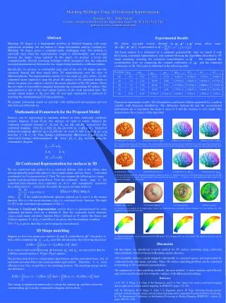
2D Strategy Schematic MOSFET geometry Boundary conditions for the Laplacian of Region 1.
Conformal mapping • To solve the Laplacian, we perform conformal mapping of region 1 into the upper half of the (u,v) complex plane (using Schwartz-Christoffel transformation) • It will be easier to find in that plane the potential distributions, because of the relative simplicity of the boundary conditions in it.
Conformal mapping Along the u-axis:
Conformal mapping • This mapping, together with some approximations, allows us to obtain an analytical expression of the component E2D(u) of the Laplacian, which results in an analytical expression of E2D(x). • Therefore, we obtain an expression of the potential distribution in the channel, which allows us to derive analytical expressions of the threshold voltage and the subthreshold current
Results (b) (a) Comparison between experimental (symbols) and modeled (solid lines) results. Bulk MOSFETs with Ns = 2x1017 cm-3 and tox = 8.6 nm (a) Threshold voltage variation with VDS (b) Threshold voltage variation with channel length at VDS=0.05 V.
Results Model calculations of the channel potential in 70 nm SSR MOSFET relative to the substrate for (a) VDS = 1.6 V at VGS = 0 V (lower curve), 0.1 V (middle curve), and 0.31 V (upper curve), Model calculations of the channel potential relative to the substrate for VDS = 0.05 V and 3 V for gate lengths of 210 nm and 250 nm and tox = 8.6 nm
Results Experimental (symbols) and modeled (lines) subthreshold transfer characteristics for a 70 nm SSR MOSFET with tox = 3nm. VDS = 0.1 V (lower curve) and 1.6 V (upper curve). Measured (symbols) and modeled (line) of the subthreshold transfer characteristic for a 250 nm MOSFET with and tox = 5.6 nm at VDS = 0.05 V.
Conclusions • We have developed a closed-form 2D modeling technique for sub-100 nm MOSFETs • The technique is based on conformal mapping, where the 2D Poisson’s equation in the depletion regions is separated into a 1D long-channel case and a 2D Laplace equation. • With a minimal parameter set, the present modeling reproduces both qualitatively and quantitatively the experimental data of deep-submicron and sub-100 nm bulk MOSFETs • Our technique can be extended to SOI MOS structures