Download
1 / 12
130 likes | 271 Vues
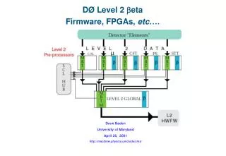
DØ Level 2 b eta Firmware, FPGAs, etc …. Drew Baden University of Maryland April 26, 2001 http://macdrew.physics.umd.edu/cms/. MBUS. Xilinx XVC405E. PLX. CPU. Overview. Goal: Interface between MBUS and PCI Implementation Single large FPGA Xilinx XCV405-EM 10,800 logic cells

E N D
DØ Level 2 beta Firmware, FPGAs, etc…. Drew Baden University of Maryland April 26, 2001 http://macdrew.physics.umd.edu/cms/
MBUS Xilinx XVC405E PLX CPU Overview • Goal: Interface between MBUS and PCI • Implementation • Single large FPGA Xilinx XCV405-EM • 10,800 logic cells • 573,440 bits true dual-port block RAM • 71,680 bytes, >4k MBUS words • 404 I/O pins (not including load, JTAG, etc.) BGA • Internal support for LVDS or PECL differential signaling @ 622 Mbps • 8 digital delay-locked loops (DLLs) per device • Eliminates clock skew for geographically separated modules • DLLs can provide 2x frequency multiplication • JTAG for boundary scans and “TAP” • Can use as an internal logic analyzer
Overview (cont) • PCI Implementation • PLX 9054 PCI bus master interface • 32bit 33MHz PCI • 2 DMA enginers • Programmable burst management • Programmable interrupt generator • 3.3V tolerant • Asynchronous local bus/PCI bus • BigLittle endian conversion • 132MB/s theoretical bandwidth • How fast can it really go? • CMS group has built a PMC card with earlier version • They got ~110MB/s DMA burst • We need around 80MB/s • MBT can probably only send ~110MB/s • Well matched
PLX 9054 • Local bus can run up to 50MHz • Has some onboard FIFOs • DMA only as a local bus master • This is ok – we can send it a message as a local bus slave to initiate DMA • Can limit this to • DMA Address • GO • DMA size • This can also be eliminated if we use fixed burst size • 3 words x 25ns (40MHz) is 75ns, very small overhead as long as DMA bursts are “large” • Ours are typically 10-20 estimated
FPGA I/O pins • 15 VME: • 9 D0 specific I/O, 6 for geographic addressing • 32 ECL scalers out • 193 MBUS: • 5 MBUS arbitration: • BOSS in, BOSS out, BOSSREQ, BOSSGRIN, BOSSGROUT • 4 MBUS handshaking • DSTROBE in, DSTROBE out, DDONE in, DDONE out • 33 MBUS address • 1 MBAD direction, 32 MBAD • 129 MBUS data • 1 MBDATA dir, 128 MBDATA • 14 MOD_DONE lines • 8 Miscellaneous • RD_WR, RD_WR_DIR, START_LOAD, DONE_OUT, MB_RESET, AP_FIFO_EMPTY, EV_LOADED(0) in and out
PLX M-mode bus J-mode is similar CCS# LCLK LFRAME# LINT# LRESETo# Add-on bus USERi USERo BB# BDIP# BG# BI# BIGEND# 89 signals BR# DP[0:3] LA[0:31] LD[0:31] MDREQ# RD/WR# RETRY# TA# TEA# TS# TSIZ[0:1] FPGA I/O pins (cont) • 19 Front panel • Clock, reset, 12 LEDs, 2 switches, 3 rotary switch • 32 Logic Analyzer test points • 89 Local Bus (aka “Add-on Bus”) Total Pin count: 380 Available on XCV405E: 404 • We will use them all, don’t worry!
Comments on 405-EM • Current MBT firmware uses 10k100+10k50 • ~8000 logic cells total • 10,800 for 405-EM – 20% more resources • Currently 33% resource utilitization. • Will probably go up to 40%, call it 50% • Supports MBUS broadcast, MBUS PIO, FIFO reading, Cypress output, L2 Global output, VME, 10k50 10k100, etc. • Functionality for Xilinx 405-EM • MBUS side: • Data FIFO load (service MBUS broadcast) • PIO • PLX side: • FIFO read • PCI DMA transfer • PCI I/O to MBUS • Conclusion: • We do not expect this firmware to require significantly more resources than for MBT – it should fit ok with resources to spare
FPGA Contingency • XCV812E • >x2 Logic Cells • x2 block RAM • x2 price! • This requires that we have a LOT of firmware simulated and synthesized this summer • This is well ahead of Sept schedule for boards • If it will not fit, we will know by Sept
Firmware • Basic firmware modules: • “Local bus” side • ORSAY • MBUS side • UMD • Interface • Joint specification • 1 week late May scheduled meeting in Paris to iron out ORSAY Maryland M B U S L O C A L B U S
Firmware Tools • HDL language • Both groups have experience in Verilog • Simulation • ORSAY uses Cadence • UMD uses Aldec • Synthesis • Agreement to both use Synplify
Manpower • Orsay • In-house experts in Verilog and Xilinx • Engineers • UMD • In-house expert in Verilog (me) • Engineers expert in FPGA schematic coding • $20k in UMD budget for engineers to contribute to firmware • Hans Breden is taking Verilog class next week • UVA • Hirosky wants to learn! • We will all remain flexible and chip in where we can • We believe we have enough manpower to succeed
Conclusions • FPGA choice is sound • Some concern in number of resources • I like to have a lot of breathing room • <50% resource utilization appears to be a good upper limit • If we need more, we need to know “now” (summer) • PLX chip is excellent • Well tested and used in industry • Same for CERN CMS group (Attila Racz, on their web site) • Manpower appears to be sufficient • Firmware functionality lends itself to separation in development • Orsay does “Local bus” side • Maryland does “MBus” side