Download
1 / 69
690 likes | 726 Vues
Learn about Charge-Coupled Devices (CCDs) and their structure, functioning, and applications in this detailed guide. Discover how CCDs convert light to electronic charge and store images on a computer. Explore the photoelectric effect, charge transfer, and potential wells in CCDs. Gain insights into the process of charge motion within CCD structures.

E N D
Introduction to CCDs Claudio Cumani Optical Detector Team - European Southern Observatory for ITMNR-5 Fifth International Topical Meeting on Neutron Radiography Technische Universität München, Garching, July 26, 2004
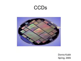
CCDs - Introduction • Charge Coupled Devices (CCDs) were invented in October 19, 1969, by William S. Boyle and George E. Smith at Bell Telephone Laboratories (“A new semiconductor device concept has been devised which shows promise of having wide application”, article on Bell System Technical Journal, 49, 587-593 (April 1970). • CCDs are electronic devices, which work by converting light into electronic charge in a silicon chip (integrated circuit). This charge is digitised and stored as an image file on a computer.
“Bucket brigade” analogy VERTICAL CONVEYOR BELTS (CCD COLUMNS) RAIN (PHOTONS) BUCKETS (PIXELS) METERING STATION (OUTPUT AMPLIFIER) HORIZONTAL CONVEYOR BELT (SERIAL REGISTER)
Conveyor belt starts turning and transfers buckets. Rain collected on the vertical conveyor is tipped into buckets on the horizontal conveyor.
Vertical conveyor stops. Horizontal conveyor starts up and tips each bucket in turn into the metering station.
After each bucket has been measured, the metering station is emptied, ready for the next bucket load. `
A new set of empty buckets is set up on the horizontal conveyor and the process is repeated.
CCD structure • A CCD is a two-dimensional array of metal-oxide-semiconductor (MOS) capacitors • The charges are stored in the depletion region of the MOS capacitors • Charges are moved in the CCD circuit by manipulating the voltages on the gates of the capacitors so as to allow the charge to spill from one capacitor to the next (thus the name “charge-coupled” device) • A charge detection amplifier detects the presence of the charge packet, providing an output voltage that can be processed • The CCD is a serial device where charge packets are read one at a time.
Charge motion Charge motion CCD structure - 1 Image area (exposed to light) Parallel (vertical) registers Pixel Serial (horizontal) register Output amplifier masked area (not exposed to light)
CCD structure - 2 Channel stops to define the columns of the image Plan View Transparent horizontal electrodes to define the pixels vertically. Also used to transfer the charge during readout One pixel Electrode Insulating oxide n-type silicon p-type silicon Cross section
Photomicrograph of a corner of an EEV CCD 160mm Image Area Serial Register Bus wires Edge of Silicon Read Out Amplifier
Full-Frame CCD Image area = parallel registers Charge motion Charge motion Masked area = serial register
Frame-Transfer CCD Storage (masked) area Image area Charge motion Serial register
Interline-Transfer CCD Image area Storage (masked) area Serial register
Basic CCD functions • Charge generation photoelectric effect • Charge collection potential well • Charge transfer potential well • Charge detection sense node capacitance
Photoelectric Effect - 1 Atoms in a silicon crystal have electrons arranged in discrete energy bands: • Valence Band • Conduction Band Conduction Band Increasing energy 1.12 eV Valence Band
Hole Electron Photoelectric Effect - 2 • The electrons in the valence band can be excited into the conduction band by heating or by the absorption of a photon photon photon
n p Potential Well - 1 Diode junction: the n-type layer contains an excess of electrons that diffuse into the p-layer. The p-layer contains an excess of holes that diffuse into the n-layer (depletion region, region where majority charges are ‘depleted’ relative to their concentrations well away from the junction’). The diffusion creates a charge imbalance and induces an internal electric field (Buried Channel). Electric potential Potential along this line shown in graph above. Cross section through the thickness of the CCD
Potential Well - 2 During integration of the image, one of the electrodes in each pixel is held at a positive potential. This further increases the potential in the silicon below that electrode and it is here that the photoelectrons are accumulated. The neighboring electrodes, with their lower potentials, act as potential barriers that define the vertical boundaries of the pixel. The horizontal boundaries are defined by the channel stops. Electric potential Region of maximum potential n p
p-type silicon n-type silicon Charge collection in a CCD - 1 Photons entering the CCD create electron-hole pairs. The electrons are then attracted towards the most positive potential in the device where they create ‘charge packets’. Each packet corresponds to one pixel pixel boundary pixel boundary incoming photons Electrode Structure Charge packet SiO2 Insulating layer
1 2 1 2 3 3 Charge transfer in a CCD +5V 0V -5V +5V 0V -5V +5V 0V -5V Time-slice shown in diagram
1 2 1 2 3 3 +5V 0V -5V +5V 0V -5V +5V 0V -5V
1 2 1 2 3 3 +5V 0V -5V +5V 0V -5V +5V 0V -5V
1 2 1 2 3 3 +5V 0V -5V +5V 0V -5V +5V 0V -5V
1 2 1 2 3 3 +5V 0V -5V +5V 0V -5V +5V 0V -5V
1 2 1 2 3 3 +5V 0V -5V +5V 0V -5V +5V 0V -5V
Performance functions • Charge generation Quantum Efficiency (QE), Dark Current • Charge collection full well capacity, pixels size, pixel uniformity, defects, diffusion (Modulation Transfer Function, MTF) • Charge transfer Charge transfer efficiency (CTE), defects • Charge detection Readout Noise (RON), linearity
Photon absorption length c: beyond this wavelength CCDs become insensitive.
(Thick) front-side illuminated CCDs • low QE (reflection and absorption of light in the surface electrodes) • No anti-reflective coating possible (for electrode structure) • Poor blue response Incoming photons p-type silicon n-type silicon Polysilicon electrodes 625 m
15m (Thin) back-side illuminated CCDs • Silicon chemically etched and polished down to a thickness of about 15microns. • Light enters from the rear and so the electrodes do not obstruct the photons. The QE can approach 100% . • Become transparent to near infra-red light and poor red response • Response can be boosted by the application of anti-reflective coating on the thinned rear-side • Expensive to produce Anti-reflective (AR) coating Incoming photons p-type silicon n-type silicon Silicon dioxide insulating layer Polysilicon electrodes