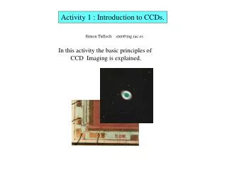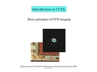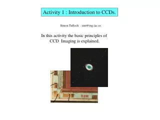
CCDs
Donna Kubik Spring, 2005. CCDs. References. 1. “Fully Depleted, Back-Illuminated Charge-Coupled Devices Fabricated on High-Resistivity Silicon”, S. E. Holland, et. al., IEEE Transactions on Electron Devices, Vol. 50, No.1, January (2003) 225-238

CCDs
E N D
Presentation Transcript
Donna Kubik Spring, 2005 CCDs
References 1. “Fully Depleted, Back-Illuminated Charge-Coupled Devices Fabricated on High-Resistivity Silicon”, S. E. Holland, et. al., IEEE Transactions on Electron Devices, Vol. 50, No.1, January (2003) 225-238 2. “Determination of the electron-hole pair creation energy for semiconductors from the spectral responsivity of photodiodes”, F. Scholze, et. al., Nuclear Instruments and Methods in Physics Research A 439 (2000) 208-215 3. CCD Astronomy, Christian Buil, Willmann-Bell, 1991 4. Scientific Charge-Coupled Devices, J. R. Janesick, Bellingham WA, SPIE Press, 2001
Charge coupled device (CCD) • The CCD was developed in 1970 by Boyle and Smith at Bell Labs • They were attempting to design a new kind of semiconductor memory for computers. • At the same time they were looking for a way to develop a solid-state camera for use in video phones.
CCDs • CCDs are dynamic devices that move charge along a predetermined paths under control of clock pulses • They now have applications in memories, logic functions, signal processing, and imaging
CCDs • Like all photodetectors, CCDs can be used to detect photons or particles • CCDs are used for astronomical imaging • CCDs can be used as particle detectors (i.e. vertex detectors)
OUTLINE • How does a CCD work? • What are the basic characteristics of a CCD? • What are the specific characteristics of the LBNL CCDs? • What about CCDs as a vertex detector for the LCD?
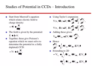
CCD structure • MOS capacitor • metal-oxide-semiconductor • Most common to use P-type substrate • Holes are majority carriers in P-type • There are a few electrons from thermal energy (minority carriers) oxide
CCD operation • Bias gate (typical 10 V) • Majority carriers (holes) are pushed back into interior of substrate • Zone almost free of majority carriers is then created at the SiO2-Si interface (depletion region) 10V oxide
Charge injection • e-h pairs created in the depletion region are separated by the potential • The e- accumulate near the SiO2-Si interface forming an n-channel • This is also called the inversion layer • The inversion layer carries the information 10V oxide
Charge transfer • After the integration time has elapsed, the charges are read out • Two phase, three phase, four phase • Example shown is the most common, three phase transfer
CCD characteristics • Quantum efficiency • Spectral response • Transfer efficiency • Spatial resolution • Linearity • Blooming • Dark current • Sensitivity to cosmic rays • Electroluminescence • Cosmetic defects • Noise
Quantum efficiency (QE) • Quantum efficiency • QE is generally <1. • QE ranges form 40% to 80% for CCDs, compared to 2% to 4% for photographic emulsion.
Detective Quantum Efficiency (DQE) • If a photon produces a photoelectron, the photoelectron will not necessarily be measured at the detector’s output. • The photoelectron could be lost in the transfer. • So another measure, equivalent quantum efficiency or detective quantum efficiency (DQE) is often used.
Charge Collection Efficiency (CCE) • QE can be > 1 for high energy photons. • For example, a thinned CCD receiving a 1216 A photon averages 3 e-h pairs. • To take this phenomenon into account, a new quality criterion was established to measure CCD performance when lit by energetic radiation (EUV and X-ray). • This is called charge collection efficiency (CCE) • SHOW GRAPH IN Scholze ARTICLE and next slide
Pair creation in Si • Pair creation energy is a function of the incident photon (or particle) energy, E • E < 1.14 eV pass through the CCD; i.e. Si is transparent in the far-infrared • 1.1 eV < E < 3.1 eV (1126 nm to 400 nm) will generate a single e-h pair • E > 3.1 eV will produce multiple e-h pairs when the energetic conduction band e- collides with other valence e- • E> 10 eV:
Hysteresis • Local variations in QE may depend on past lighting (hysteresis). • If the CCD was recently lit by intense light, those areas that were strongly lit have higher QE. • To minimize this effect, can illuminate the entire array with a 700 nm source and then take many rapid readouts prior to exposure.
Spectral response • Spectral response close to that of Si. • Without any special “tinkering”, the spectral response is close to that of Si; the CCD can usually record radiation form 0.4 um to 1 um. • The possibility of recording information beyond 0.7 um is new and important, for the eye and photographic plates are insensitive beyond that limit. • The spectral sensitivity may also vary from pixel to pixel.
Transfer efficiency • During the transfer from one stage to another, a certain number of charges is left behind • A measure of the efficiency is termed charge transfer efficiency (CTE)
Transfer efficiency • Only a slight inefficiency is tolerable • If 1% of the charges is left behind after each transfer, a packet initially containing 100 electrons will contain only 37 electrons • Today’s large arrays, a packet must be moved an average of 500 times! • CCD mfg are trying to reach a near-perfect rate • Typical efficiency is 0.999990
Transfer efficiency • CTE = f(temperature) • It temperature is too low, carrier mobility decreases and blocks operation of the CCD • CTE = f(clock rate) • In astrononmy, it is always possible to read the CCD slowly • CTE = f(number of charges) • If <1000 e-, noticeable trapping • Pro: Saturate traps with LED flash (thermal current can also do this if only moderately cooled) • Con: Adds noise
Spatial resolution • Pixels 10-30 um long • Compare to 5 um grain size in emulsion • Transfer inefficiency can dilute the charges of a pixel into the following pixels • Diffusion of charges in substrate during integration • Especially for long wavelengths which have longer absorption lengths • Solution is to thin the P doped layer (substrate) so that they recombine in the supporting substrate • But this decreases red sensitivity
Linearity • The linearity of a CCD is very good • Linearity is limited to a working range of intensity • For low illumination, linearity is no longer possible because of threshold phenomena, as charge trapping • At high light levels, the detector becomes saturated • Space charge occurs in which e- repel each other an leak over into adjacent pixels causing blooming (next slide)
Blooming vs. antiblooming • Anti-blooming gate designed to bleed off overflow from a saturated pixel. • Without this feature, a bright star which has saturated the pixels will cause a vertical streak. Example of blooming
Dark Current • Even if the CCD is in complete darkness, a signal is observable • The signal is due to thermally created charges • Main reason to cool a CCD is to minimize the dark current • Production rate is such that, at room temperature, a standard CCD in darkness is saturated after only a few seconds of integration • Dark current becomes nearly negligible at about -100 deg C • Thermal signal decreases by a factor of 2 for a 7 deg C drop in operating temperature
Dark Current • But if a CCD is cooled to a very low temperature, the Si characteristics change • In practice, a CCD is never cooled below -120 deg C • Decreased mobility • At low temperatures, the spectral sensitivity changes • A shift toward blue on the infrared side of response curve • Typical 2.5 Angstroms/deg C • The thermal current comes from the Si-SiO2 interface, so designers are trying to build CCDs where this effect is minimized (MPP, multi-pinned phase)
Sensitivity to cosmic rays • Cosmic rays can interact with Si • If it arrives on an angle, would leave a streak • Increased problem at high altitudes and in space • Can discriminate CR by comparing images of same field Cosmic ray
Electroluminescence • The output amplifier can emit a weak light by electroluminescence • Solution is to turn off or lower amplifier voltage during exposure and then just turn it on immediately before readout
Cosmetic defects • A cosmetic defect is any defect locally affecting the quality of the sensitive surface • Some pixels may have greater dark current than their neighbors (hot spots), a complexly insensitive pixel (dark spot), or sometimes a defective column. • Most CCDs have some defects • Mfg offer several levels of quality • 5 or 6 bad pixels uniformily distributed in an image or even a defective column can be tolerated and corrected during image processing
Noise • There are many sources of noise • Thermal • Reset noise • Phonon (shot) noise • Readout noise
Correlated double sampling (CDS) • Correlated double sampling yields the best representation of the true charge associated with each pixel • From an electronics standpoint, there are different methods for accomplishing this, such as digital, analog sample and hold, integration, and dual slope.
Correlated double sampling (CDS) • Before the charge of each pixel is transferred to the output node of the CCD, the output node is reset to a reference value • The pixel charge is then transferred to the output node. The final value of charge assigned to this pixel is the difference between the reference value and the transferred charge
Dark noise • Although the dark count can be subtracted, the dark noise cannot. The dark noise is approximately the square root of the dark count. In this example, the dark noise is about 55 electrons.
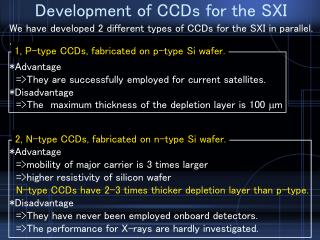
Astronomical imaging • LBNL has developed red-extended CCDs for high redshift surveys (Supernovae Cosmology Project, SNAP, DES) • Extended red response is extremely important due to the use of distant, high redshift supernovae for the determination of cosmological parameters and for deep surveys • Detection and follow-up spectroscopy of high redshift objects would greatly benefit from CCDs with improved near-infrared response.
Astronomical imaging • The large focal planes of astronomical telescopes require high-QE, large-format CCD detectors. • In order to achieve high QE, the standard scientific CCD is thinned and back illuminated
Frontside vs.backside • Back-illuminated CCDs have exceptional quantum efficiency compared to front-illuminated CCDs • To make a back illuminated CCD, take a front-illuminated CCD, thin it to ~20 µm, and mount it upside down on a rigid substrate • The incoming light now has a clear shot at the pixel wells without the gate structures blocking the light
Thinning • Thinning is required, because the relatively low-resistivity silicon used to fabricate scientific CCDs limits the depth of the depletion region. • If left thick, the shorter- wavelength, short absorption- length photons will be absorbed before reaching the depletion region where the e-h pairs they create are more efficiently collected
Back-illumination • However, this process degrades red and near-infrared responses due to the rapid increase in absorption length in silicon at long wavelengths (next slide) • In addition, fringing patterns due to multiply-reflected light are observed in uniformly illuminated images taken at near-infrared wavelengths where the absorption length exceeds the CCD thickness. • Absorption length is the reciprocal of the absorption coefficient (next slide) Typical Q.E. curves for front- and back-illuminated CCDs
Absorption coefficient • The intensity of the photon flux, F, varies as a function of the thickness, z, of the silicon, following the relation where ais the coefficient of intrinsic absorption of the silicon and F(0) is the incident flux on the silicon. Note: Energy (eV)
Absorption length • 90% of the radiation penetrating the Si is absorbed after a distance
Absorption length • Notice that blue photons (400 nm) are stopped at less than 1 um, while infrared photons (1000 nm) can cover more than 100 um. • Also note less temperature dependence at shorter wavelengths
Absorption length • Si is an indirect-bandgap semiconductor, therefore two regimes can be seen with change occurring at about 2.5 eV (500 nm) • The direct bandgap energy of Si is 2.5 eV • The indirect bandgap energy of Si is 1.12 eV • Above 2.5 eV, the transitions are direct • Below 2.5 eV, the transitions are indirect
Direct vs. indirect bandgap materials phonon Indirect gap Ge is a direct bandgap material Si is an indirect bandgap material
Direct vs. indirect transitions in Si • Above 2.5 eV, the transitions are direct • Below 2.5 eV, the transitions are indirect phonon Si is an indirect bandgap material
Direct transitions • For photon energies above 2.5 eV, absorption is highly efficient and the absorption coefficient is determined by available conduction band states. • Absorption coefficient for direct transitions, ad, varies as square root of energy as per the energy dependence of the conduction band density of states • Temperature dependence is weak in direct bandgap regime Direct
Indirect transitions • Below 2.5 eV, phonons are required for momentum conservation • Absorption less efficient • More sensitive to temperature due to phonon statistics • Absorption coefficient for indirect transitions, ai • The 2 terms are due to phonon absorption and emission Indirect
Astronomical imaging • The CCD developed by LBNL achieves high QE in the red and near-infrared by using a thick depleted region made possible by the use of a high-resistivity silicon substrate • The high resistivity allows for fully-depleted operation (200-300um) at reasonable voltages
QE of LBNL CCD Typical Q.E. curves for front- and back-illuminated CCDs Much-improved IR sensitivity LBNL CCD QE
Drawbacks of thick CCDs • There are several drawbacks to a thick CCD • Cosmic ray and terrestrial radiatoon sources will affect more pixels (more volume) • More volume for dark current • Depth of focus issues • Light incident at large angles from the normal
LBNL remedies to drawbacks • LBNL CCD is p-channel (due to LBNO experience with fabrication low dark current p-i-n diodes) • Few e-/hour • Degraded readout speed due to the lower mobility in p-channel is not of a concern for astronomy applications due to relatively low readout rates • P-channel under study for space applications due to expected higher resistance to cosmic ray protons