Download
1 / 22
230 likes | 405 Vues
A brief overview of the ATLAS Pixel Detector. Overview. It will (try) to give a brief overview over the layout, components and status of the Atlas Pixel system Layout Modules Sensors and chip Staves Support structure and integration

E N D
Overview • It will (try) to give a brief overview over the layout, components and status of the Atlas Pixel system • Layout • Modules • Sensors and chip • Staves • Support structure and integration • Many thanks to the ATLAS Pixel Community for providing the information presented here • The Atlas Pixel Detector Project is a collaboration of 23 institutes • In particular Chiara Meroni / INFN Milano and Kevin Einsweiler / LBL
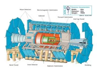
Radiation hardness: NIEL > 1015 1 MeV neq/cm2 500 kGy Operates inside the 2T field Cooled by C3F8 evaporative system . Environmental temperature kept below 0C. ~380 mm ~1.3 m The ATLAS Pixel Detector • Vertex detector to provide 3 space points • RF resolution ~ 13mm • Pixel size 50x400mm • based on 3 barrel layers (innermost is at R=5.1cm) + 2 endcaps with 3 layers each • Coverage is up to |h|<2.5
Layout • Barrel layers build out of 112 staves (1456 modules) and EC out of disks (288 EC module total) • Total of 1.8m2 and 80 MPixel • Operates at 2V with ~3500A supplied to FE
The module • It consists of a silicon sensor read-out by 16 front-end (FE) chips connected via bump bonding • 46k channels / module • Self-contained unit controlled by a Module Controller Chip, which also performs the event building. • All communications use low voltage differential signal on micro-cables before being converted in optical signals at the end of the whole pixel detector active area, Opto Board. Module Controller Chip Flex hybrid Sensor 16 FE chips Pigtail HV connection
The Sensors • Sensors are required to (also) operate under-depleted (max. operating bias 600V). Use oxygenated n-in-n sensors with pixel insulated by a moderate p-spray implant • A bias grid is used to keep pixel at equipotential during sensor testing (thickness = 280 mm) • Implemented ganged pixels to avoid dead areas between chips • Production finished at CiS/Germany and ON Semiconductor (TESLA), Czech Republic.
The front-electronics chip, FE-I3, is built in 0.25 m IBM technology: Each chip reads out 2880 pixels (7.4x11mm die). Each pixel cell consists of a fast preamplifier followed by a discriminator sparse readout and store hits in EndOfColumn buffers until the level 1 trigger is received Threshold can be adjusted by a 7-bit tuning DAC in each channel. 8-bit pulse height information is obtained by the Time-over-Threshold technique. ToT uniformity is obtained by a 3-bit tuning DAC On wafer testing measured yield is 81% Production finished ( >45000 chip) The rad-hard FE readout • For a module noise is typically : • 150 e for standard pixels • 270 e for ganged pixels • After irradiation, it is ~ 250 e (increased leakage current)
AMS - In IZM – PbSn Bump bonding • Two techniques, from different manufacturers have been used for production modules: • In bumps by Selex (ex Alenia-Marconi Systems), Rome • PbSn bumps by Fraunhofer-Institut für Zuverlässigkeit und Mikrointegration, Berlin • Bumping defects can be investigated by X-ray inspections, or electrical tests, and now are very rare: the production contract fixes a rejection ratio of 150 faulty bumps/modules (0.3%).
Some testbeam results • Module tested in PS before and after irradiation • efficiency(TDR requirement >97%): • >99.9% before irradiation • 97.8% after irradiation (@500V, already fully depleted) • signal after irradiation ~15k e- @600V • resolution(TDR requirement < 13 m): • 7.5 m at 10° incidence before irradiation, • 9.7 m at 15° incidence after irradiation, • Modules also tested with LHC-like particle flux • Check readout achitecture • Verify that efficiency is ok at LHC-like occupancy In-time efficiency as function of Time -> plateau of 10ns width
Production testing • Module performance is tested using internal calibration circuit • Measure threshold and noise by injecting 200 different values ToT for 1 pixel
Module production is almost finished: need is 1744 modules Production yield is ~ 93% Modules are ranked to install the best on the B-layer and disk1, ranking =60 0.1% of dead pixel Module Production Status as of May 2006
Integration of the Pixel Detector • Sequence of integration • Modules, after tests, are glued on CC support ladder which includes cooling pipe (13/stave) • Staves are cabled and retested • 2 staves are inter connected with cooling pipe and mounted on support half shells • Support half-shells and then surveyed and service panels installed which include the opto-boards and all services to the end of the pixel detector package • Halfshells integrated around beam pipe in cleanroom on the surface (ATLAS SR1) and installed in a single support tube. • The complete Pixel detector with beam pipe is brought to the pit and installed as the last part the Inner Detector
Structure • ~7m structure (all in CF, CC composite) with halfshells place in global support structure
The Endcaps Sector assembly (1/8 of a disk): 6 modules are mounted on carbon-carbon plates, sandwiching the cooling pipe. All 6 disks have been assembled in LBL and ENDCAP C is now at CERN Will be used for a first commissioning of the Pixel Detector using a cosmic setup in SR1
L2 Layer L1 Layer B Layer The Barrels • Stave consists of 13 modules on CF ladder which includes the Al cooling pipe • The barrel frame, made of carbon fiber laminate will hold the staves • Most staves at CERN now and are currently being cabled and made to bi-staves
Staves in halfshells • Started with integration of bi-staves on halfshells (main activity during and after summer)
Summary • Production of modules finished now and tests show that they perform as required • All pixel disks and most staves produced by ow • Focus is now on integration of staves to halfshells and halfshells together • In parallel a lot of emphasis is given to service installation and integration of off-detector systems (DAQ, DCS, PS, cooling) • Plan to install pixel system in ATLAS in March 2007 ready for commissioning with the ID and ATLAS A 3 hit Pixel Detector is on its way to record LHC events in ATLAS
Rad-hard sensors • External pixel layers will receive a yearly damage from NIEL corresponding to a fluence of 1014 neq/cm2 • B-layer at R=5.5 cm will be a factor two more. • Initial specification were: • external layers must withstand 10 years of operation at the LHC • B-layer must withstand at least 5 years of operation • That means: • NIEL >1015 neq/cm2 • dose > 500 kGy Oxygenated FZ silicon was chosen because of improved hardness to charge particle irradiation.
No. of transistors: 880 k Dimensions: 6840 x 5140 mm2 MCC-I2 Module Controller (MCC) and hybrid • Validated SEU resistance : • all critical registers are tripled and use a majority decision logic; • in the FIFO’s, where data are stored, a bit-flip safe encoding is used to unambiguously disentangle hits (for which a small corruption rate is acceptable) from event separators (whose loss would cause DAQ misalignment) • At the PS irradiation facilities MCC were run for the equivalent of 100000 s at the B-layer, without the need to reconfigure the chip. • The MCC and decoupling capacitors, temperature sensors and resistors needed by the LVDS buffers, are mounted on flex hybrids (Dyconex, CH) which are glued on the backside of the sensors • Shown is the support card used for module charactherization.
Problem during stave production found • After 30% of stave production, significant leaks found in the end regions of some staves initiated a deep investigation. Leaks and corrosion were found even in the middle of some stave. The origin was in the brazing of the cooling fitting followed by not accurate enough QC procedure • Strategy to recover was following a triple path: • Insertion of a new pipe in the already loaded stave to restore integrity, after cleaning and passivating the existing corroding pipe. • Repair: replace the present cooling pipe with a new pipe, via a controlled delamination of carbon-carbon structure and a subsequent re-assembly. • New Staves: to compensate for the losses • All need new cooling tubes and fitting • After a very dedicated effort , the stave production resumed • Full support from ATLAS that modified the schedule to delay the Pixel insertion to the very last moment (03/07)