Download
1 / 1
10 likes | 145 Vues
A Readout System Utilizing the APV25 ASIC for the Forward GEM Tracker in STAR. G. J. Visser 1 , J. T. Anderson 2 , B. Buck 3 , A. S. Kreps 2 , T. Ljubicic 4 1 Indiana University Center for Exploration of Energy and Matter, USA 2 Argonne National Laboratory, USA

E N D
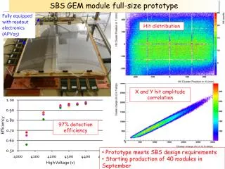
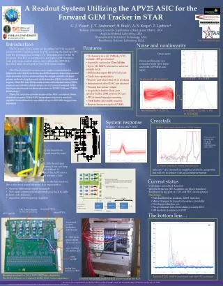
A Readout System Utilizing the APV25 ASIC for the Forward GEM Tracker in STAR G. J. Visser1, J. T. Anderson2, B. Buck3, A. S. Kreps2, T. Ljubicic4 1Indiana University Center for Exploration of Energy and Matter, USA 2Argonne National Laboratory, USA 3Massachusetts Instituteof Technology, USA 4Brookhaven National Laboratory, USA http://www.star.bnl.gov/ Introduction The Forward GEM Tracker (to be online for FY12 run) will extend STAR’s tracking reach to η=2 , covering the Endcap EMC, with the principal focus being e+/e− discrimination for the W program. The FGT is comprised of six triple GEM chambers with pad/strip readout planes, and utilizes the APV25-S1 frontend ASIC developed for theCMS silicon tracker. The GlueX detector system, now under construction for Jefferson Lab Hall D includes the 3098 channel straw tube central drift chamber (CDC) surrounding the target, and the 24 layer planar cathode strip forward drift chamber (FDC) in the forward region. The FDC has 2304 anode wires with discriminator/TDC readout and 10368 cathode strips. An 8 channel frontend ASIC has been developed for these detectors in TSMC 0.25 µm CMOS technology.† The CDC and the cathode strips of the FDC, a total of 13466 channels, require 12 bit ADC (waveform digitizer) readout capable of deadtimeless operation at up to 200 kHz trigger rate, blahblah Noise and nonlinearity Features Open input: • 72 channels in a 6U VME64x/VXS module, $55 per channel • Assembly option for 12 or 14 bits • Up to 125 MSPS, internal or external sample clock • Differential input 440 mV full scale • Cable loss equalization • Shaper/anti-alias filter 24 ns peaking • Independent offset DAC per channel • Preamp test pulser output • Acquisition buffer: Dual-port circular buffer, 2048 points (19.5 μs) • FPGA-based signal processing • 1 MB buffer and 2eSST readout • Remote firmware upload (VME) Noise and linearity are evaluated with open input and with 14.9 MHz sine input. σ = 0.52 σ = 0.43 Single event 1000 pt readout σ = 5.62 (12-bit: 1.40) 11.5 ENOB Nonlinearity ≈ 0.05 % Receiver / freq eq. Crosstalk System response Preamp + 18 m cable + ADC Shaper 15 MHz* sine input, single event 100 pt readout DAC per channel ADC *Corresponds to peaking time ≈33 ns for combined system (preamp, cable, ADC) THERE ARE MANY ELEMENTS OF OLD POSTER HERE STILL TO BE CHANGED/DELETED!! • Design choices • Some compromises are necessary for maximum channel density. The analog signal path must be kept relatively simple. • In particular: • A passive shaper uses no power, little board area • An ADC driver stage is not necessary if we can keep the drive impedance reasonably low without it • Differential drive is not necessary if the ADC uses a (relatively) high VDD and if we can tolerate a little nonlinearity • However we do not compromise on the line receiver, this is the most crucial element. It is important to: • Receive differential signal accurately • Not inject common-mode ground noise back to cable & front end electronics • Equalize cable frequency response 21 hostile (red) and 1 hostile (blue & brown) Indicates ~2% crosstalk in neighbor channels, acceptable but will try to reduce with layout improvements Mezzanine board Main board ADC FE FIFO ADC FE FIFO ADC FE FIFO • Current status • 3 modules assembled & tested • Interim firmware (FE deadtime, no block transfers) • Deployed in support of CDC and FDC development • Next steps: • Full deadtimeless readout, 2eSST transfers • Minor changed to layout (obsolence, crosstalk) • Develop production test • Pre-production run (20 modules) in early 2011 • 188 modules (+spares) in 2012 FE (Front-end processing): This includes acquisition buffer writing, point extraction, lookahead zero suppression, channel number & header insertion ADC FE FIFO … (36 ch total) … … (36 ch total) … Channel data FIFO: 1024 words (16 bits + 2 flags, internal use only) ADC FE FIFO ADC FE FIFO ADC FE FIFO ADC FE FIFO ADC FE FIFO ADC FE FIFO Each 160 MB/s i.e. 400 words/evt @ 200 kHz 320 MB/s 1 MB Frontend FPGA XC3S500E-4 12 total, 6 ch each Processor FPGA Output FIFO VME slave 2eSST etc. frontend FPGA FEE Power Supply ±1.8V 2.5A remote reg. XC3SD3400A-4 160 MB/s main FPGA ADC (quad) The bottom line… to readout / control backplane (CPCI style) 0 – 360° clock phase shifter (4×) for APV & ADC opto-isolated I2C master (2×) cable to FEE analog line receiver / filter Readout module for 2×12 APV (3072 det. channels) The PCB is 10 layers w/ 6 planes (3 GND), 0.003” buried capacitance. Typical FDC event (preliminary data from FDC prototype) Complete integrated readout and power system for FGT This work was supported in part by the Offices of NP and HEP within the U.S. DOE Office of Science and by the U.S. NSF. †GAS II: A Versatile Wire Chamber Readout ASIC. N. Dressnandt, N. Doshi, M. Newcomer., IEEE NSS 2009.