Download
1 / 26
280 likes | 876 Vues
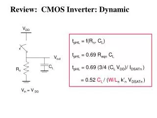
C L. Review: CMOS Inverter: Dynamic. V DD. t pHL = f(R n , C L ) t pHL = 0.69 R eqn C L t pHL = 0.69 (3/4 ( C L V DD )/ I DSATn ) = 0.5 2 C L / ( W/L n k’ n V DSATn ). V out. R n. V in = V DD. Review: Designing Inverters for Performance. Reduce C L

E N D
CL Review: CMOS Inverter: Dynamic VDD tpHL = f(Rn, CL) tpHL = 0.69 Reqn CL tpHL= 0.69 (3/4 (CL VDD)/ IDSATn ) = 0.52 CL/ (W/Ln k’n VDSATn ) Vout Rn Vin = V DD
Review: Designing Inverters for Performance • Reduce CL • internal diffusion capacitance of the gate itself • interconnect capacitance • fanout • Increase W/L ratio of the transistor • the most powerful and effective performance optimization tool in the hands of the designer • watch out for self-loading! • Increase VDD • only minimal improvement in performance at the cost of increased energy dissipation • Slope engineering - keeping signal rise and fall times smaller than or equal to the gate propagation delays and of approximately equal values • good for performance • good for power consumption
Rp Rp Rp Rp Rp Rp A B A A B A Rn Cint Cint CL CL CL Rn Rn Rn Rn A B A A B NOR NAND Switch Delay Model Req A A INVERTER
Rp Rp B A Cint CL Rn B Input Pattern Effects on Delay • Delay is dependent on the pattern of inputs • Low to high transition • both inputs go low • delay is 0.69 Rp/2 CL since two p-resistors are on in parallel • one input goes low • delay is 0.69 Rp CL • High to low transition • both inputs go high • delay is 0.69 2Rn CL • Adding transistors in series (without sizing) slows down the circuit Rn A
Delay Dependence on Input Patterns 2-input NAND with NMOS = 0.5m/0.25 m PMOS = 0.75m/0.25 m CL = 10 fF A=B=10 A=1 0, B=1 A=1, B=10 Voltage, V time, psec
Rp Rp Rp Rp A B A B Rn Cint Cint CL CL Rn Rn Rn B A A B Transistor Sizing 2 2 1 1 2 2 1 1
A D Transistor Sizing a Complex CMOS Gate B 4 12 2 6 C 4 12 2 6 OUT = !(D + A • (B + C)) A 2 D 1 B 2 C 2
D C B A C3 C2 C1 CL Fan-In Considerations A B Distributed RC model (Elmore delay) tpHL = 0.69 Reqn(C1+2C2+3C3+4CL) Propagation delay deteriorates rapidly as a function of fan-in – quadratically in the worst case. C D
tp as a Function of Fan-In quadratic function of fan-in tp (psec) tpHL tp tpLH linear function of fan-in fan-in • Gates with a fan-in greater than 4 should be avoided.
C3 C2 C1 CL Fast Complex Gates: Design Technique 1 • Transistor sizing • as long as fan-out capacitance dominates • Progressive sizing Distributed RC line M1 > M2 > M3 > … > MN (the fet closest to the output should be the smallest) InN MN In3 M3 In2 M2 Can reduce delay by more than 20%; decreasing gains as technology shrinks In1 M1
C2 C1 C1 C2 CL CL Fast Complex Gates: Design Technique 2 • Input re-ordering • when not all inputs arrive at the same time critical path critical path 01 charged charged 1 In1 In3 M3 M3 1 1 In2 In2 M2 discharged M2 charged 1 In3 discharged In1 charged M1 M1 01 delay determined by time to discharge CL, C1 and C2 delay determined by time to discharge CL
D C B A C3 C2 C1 CL Sizing and Ordering Effects 3 3 3 3 A 4 4 = 100 fF B 4 5 Progressive sizing in pull-down chain gives up to a 23% improvement. Input ordering saves 5% critical path A – 23% critical path D – 17% C 4 6 D 4 7
Fast Complex Gates: Design Technique 3 • Alternative logic structures F = ABCDEFGH
CL CL Fast Complex Gates: Design Technique 4 • Isolating fan-in from fan-out using buffer insertion • Real lesson is that optimizing the propagation delay of a gate in isolation is misguided.
Design Technique 5 - Logical Effort • The optimum fan-out for a chain of N inverters driving a load CL is f = (CL/Cin) • so, if we can, keep the fan-out per stage around 4. • Can the same approach (logical effort) be used for any combinational circuit? • For a complex gate, we expand the inverter equation tp = tp0 (1 + Cext/ Cg) = tp0 (1 + f/) to tp = tp0 (p + g f/) • tp0 is the intrinsic delay of an inverter • f is the effective fan-out (Cext/Cg) – also called the electrical effort • p is the ratio of the instrinsic (unloaded) delay of the complex gate and a simple inverter (a function of the gate topology and layout style) • g is the logical effort N
Intrinsic Delay Term, p • The more involved the structure of the complex gate, the higher the intrinsic delay compared to an inverter Ignoring second order effects such as internal node capacitances
Logical Effort Term, g • g represents the fact that, for a given load, complex gates have to work harder than an inverter to produce a similar (speed) response • the logical effort of a gate tells how much worse it is at producing an output current than an inverter (how much more input capacitance a gate presents to deliver it same output current)
B A B A A A + B A • B A A A A B B Example of Logical Effort • Assuming a pmos/nmos ratio of 2, the input capacitance of a minimum-sized inverter is three times the gate capacitance of a minimum-sized nmos (Cunit) 4 2 2 2 4 1 2 2 1 1 Cunit = 3 Cunit = 4 Cunit = 5
effort delay intrinsic delay Delay as a Function of Fan-Out • The slope of the line is the logical effort of the gate • The y-axis intercept is the intrinsic delay NAND2: g=4/3, p = 2 INV: g=1, p=1 normalized delay • Can adjust the delay by adjusting the effective fan-out (by sizing) or by choosing a gate with a different logical effort • Gate effort: h = fg fan-out f
CL Path Delay of Complex Logic Gate Network • Total path delay through a combinational logic block tp = tp,j = tp0 (pj + (fj gj)/ ) • So, the minimum delay through the path determines that each stage should bear the same gate effort f1g1 = f2g2 = . . . = fNgN • Consider optimizing the delay through the logic network how do we determine a, b, and c sizes? 1 c b a 5
Path Delay Equation Derivation • The pathlogical effort, G = gi • And the path effective fan-out (path electrical effort) is F = CL/g1 • The branching effort accounts for fan-out to other gates in the network b = (Con-path + Coff-path)/Con-path • The path branching effort is then B = bi • And the total path effort is then H = GFB • So, the minimum delay through the path is D = tp0 ( pj + (N H)/ ) N
CL Path Delay of Complex Logic Gates, con’t • For gate i in the chain, its size is determined by si = (g1 s1)/gi (fj/bj) i-1 j=1 1 c b a 5 • For this network • F = CL/Cg1 = 5 • G = 1 x 5/3 x 5/3 x 1 = 25/9 • B = 1 (no branching) • H = GFB = 125/9, so the optimal stage effort is H = 1.93 • Fan-out factors are f1=1.93, f2=1.93 x 3/5 = 1.16, f3 = 1.16, f4 = 1.93 • So the gate sizes are a = f1g1/g2 = 1.16, b = f1f2g1/g3 = 1.34 and c = f1f2f3g1/g4 = 2.60 4
Fast Complex Gates: Design Technique 6 • Reducing the voltage swing • linear reduction in delay • also reduces power consumption • requires use of “sense amplifiers” on the receiving end to restore the signal level (will look at their design when covering memory design) tpHL= 0.69 (3/4 (CL VDD)/ IDSATn ) = 0.69 (3/4 (CL Vswing)/ IDSATn )
TG Logic Performance • Effective resistance of the TG is modeled as a parallel connection of Rp (= (VDD – Vout)/(-IDp)) and Rn (=VDD– Vout)/IDn) W/Lp=0.50/0.25 0V Rn Rp 2.5V Vout Rp Rn Resistance, k 2.5V Req = Rn || Rp W/Ln=0.50/0.25 Vout, V • So, the assumption that the TG switch has a constant resistive value, Req, is acceptable
0 0 0 0 5 5 5 5 Vin Req Req Req Req V1 Vi Vi+1 VN C C C C • Delay of the RC chain (N TG’s in series) is tp(Vn) = 0.69 kCReq = 0.69 CReq (N(N+1))/2 0.35 CReqN2 N k=1 Delay of a TG Chain Vin V1 Vi Vi+1 VN C C C C
0 0 0 0 0 5 5 5 5 5 M 0 VN Vin C C C C C 5 TG Delay Optimization • Can speed it up by inserting buffers every M switches • Delay of buffered chain (M TG’s between buffer) tp = 0.69 N/M CReq (M(M+1))/2 + (N/M - 1) tpbuf Mopt = 1.7 (tpbuf/CReq ) 3 or 4