The RC Delay Model for Gates
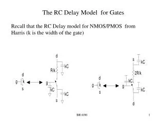
The RC Delay Model for Gates. Recall that the RC Delay model for NMOS/PMOS from Harris (k is the width of the gate). General RC Inverter Model. Inverter Model. Rui : pullup resistance. Rui. in. out. Cpi. Cout. Cin. Rdi. Rdi : pulldown resistance.

The RC Delay Model for Gates
E N D
Presentation Transcript
The RC Delay Model for Gates Recall that the RC Delay model for NMOS/PMOS from Harris (k is the width of the gate) BR 6/00
General RC Inverter Model Inverter Model Rui : pullup resistance Rui in out Cpi Cout Cin Rdi Rdi : pulldown resistance Cpi: parasitic cap of gate from drain capacitances BR 6/00
Inverter RC Delay Model Tplh (pullup delay) = Rui * ( Cpi + Cout) = Rui * Cpi + Rui * Cout = parasitic delay PU + load delay PU Tphl (pulldown delay) = Rdi * ( Cpi + Cout) = Rdi * Cpi + Rui * Cout = parasitic delay PD + load delay PD BR 6/00
Parasitic Delay versus Load Delay Parasitic delay is fairly constant with increasing gate width because the channel resistance goes down with increasing Width, but the drain capacitance goes up, so the total R*C is about constant. Load delay is proportional to Cout/Cin because wider transistors (increasing Cin) can drive a fixed output load faster, while an increasing load causes a larger gate delay for a fixed driving transistor width. BR 6/00
Measuring Delay, Ri, Cpi a. If you measure delay for NO-LOAD, then you get the no-load delay. b. Add a fixed load, then measure the delay. Subtract the no-load delay, and you get the load delay. c. The load capacitance can be measured since it is a static value. Once the load capacitance is known, you can calculate the Ri value. Once the Ri value is known, you can calculate the Cpi value. BR 6/00
Delay Measurement We will use 30% to 70% points for delay measurement, but 50%-50% can also be used. BR 6/00
Improving Average Delay† A question: Should the DC switching point of a static CMOS gate always be set at Vdd/2? Recall the DC switching characteristic of a static Inverter Normal Skew, balanced Tplh, Tphl Vin Increasing P/N ratios Vdd/2 High Skew (4/1) favors rising outputs,decreased Tplh low Skew (1/1) favors falling outputs, decreased Tphl Vdd/2 Vout BR 6/00 †Harris ’97 Notes for these slides
2/1 4/1 1/1 2/2 4/2 1/2 4/1 8/1 2/1 Gate Sizes and Skew Normal Skew High Skew Low Skew Use skewed gates when trying to speed up a particular output transition along a critical path. BR 6/00
Minimum Average Delay What should the skew be to minimize average delay in a string of inverters driving a load? Consider one inverter driving a fanout f load. (Cin of inverter = 1 + ) (width) f*(1+ ) 1 BR 6/00
Minimum Average Delay (cont) Average delay = (Tplh + Tphl)/2 Recall RC model time model: Tp = Tnoload + K*Cload where is K is inversely proportional to channel width (represents channel resistance). We can ignore Tnoload for this analysis. Tphl (falling delay) proportional to 1*f (1 + ) Tplh (rising delay) proportional to k/ *f (1 + ) where ‘k = B’ for the case of Tplh = Tphl. ‘k’ accounts for differences in P/N mobility. BR 6/00
1.4/1 Minimum Average Delay (cont) Average delay = (Tplh + Tphl)/2 = (k/ *f (1 + ) + f (1 + ) )/2 = f (1 + ) (k/ + 1)/2 To find best value for , take derivative and set to 0: d delay/d = f/2 (1 - k/2) = 0 = sq_root(k ) !!! Minimum average delay Trades off some Tplh time for overall decreased loading. Saves power as well! BR 6/00
1.4/1 2/2 2/1 Minimum Average Delay Min average delay These gates sized for minimum average delay. BR 6/00
Topology Selection Which is better? We have seen that logical effort may be able to help us make this choice, but usually simulation is needed. Right choice is technology dependent!!!! Cin=C 8C Option #1 8C Option #2 BR 6/00
A A A A B B B B Co Co Co Co Ci Ci Ci Ci S S S S Critical Inputs In general, late arriving inputs should drive inputs that are close to the output, early arriving inputs should drive inputs that are close to the rail. For example – in a full adder cell, carry input should be close to output (Fig 11-6 pg 567, Rabaey). 4-bit ripple adder. A(3) B(3) A(2) B(2) A(1) B(1) A(0) B(0) Cout C(4) C(3) C(2) C(1) C(0) Cin Sum(3) Sum(2) Sum(1) Sum(0) BR 6/00
If Arrival times are unknown.... If arrival times are unknown, and you need to fold the transistors anyway, can use the following trick: BR 6/00
Stack Tapering Increasing width of transistors near rail can improve delay. Benefits at sub-micron geometries are somewhat marginal. BR 6/00
Summary of Static CMOS Features • Very robust – i.e, “almost idiotproof” (Harris quote!) • Very low DC leakage (nearly zero) • Low AC power • Scales well to low voltage • Handled well by synthesis tools and simulators • Well understood Should be the default case for logic implementation unless special needs dictate some other family. BR 6/00