Download
1 / 35
360 likes | 599 Vues
Photovoltaics. F.-J. Haug Ecole Polytechnique Fédérale de Lausanne (EPFL), Institute of Microengineering (IMT), Photovoltaics and Thin Film Electronics Laboratory (PV-Lab), 2000 Neuchâtel, Switzerland. Outline. Why Solar Cells? How do they work? Why thin film silicon solar cells?

E N D
Photovoltaics F.-J. Haug EcolePolytechniqueFédérale de Lausanne (EPFL), Institute of Microengineering (IMT), Photovoltaics and Thin Film Electronics Laboratory (PV-Lab), 2000 Neuchâtel, Switzerland.
Outline • Why Solar Cells? • How do they work? • Why thin film silicon solar cells? • What do we do at PV-Lab? • thin film solar cells on glass and plastic substrates • thin films for wafer-based cells (hetero-junction cells) • transparent conducting oxides • (sensor applications) • (module design and reliability) F.-J. Haug – Photovoltaics
The power source: Our Sun • A low to medium size star • Heated by fusion(essentially , processes for , etc.) • Power output: (convert to energy) • Delivers to the earth • 10’000 the global energy consumption F.-J. Haug – Photovoltaics
Solar irradiation atlas Central Europe: ca 1 kW/m2 under clear sky at noon Yearly average: 1000 kWh/m2, ca 3 hours every day SolarGIS F.-J. Haug – Photovoltaics
The solar spectrum • The solar spectrum resembles white-hot body glowing at T=5700 K • Usually measured with respect to wavelength (use a grating or a prism) • In PV: often necessary to convert to photon energy: See www.pvlighthouse.com.au F.-J. Haug – Photovoltaics
Filtering by atmosphere: air mass (AM) AM0: space integrated: 1366 W/m2 AM1: equator AM1.5: central Europe 1000 W/m2 AM2: 30° above horizon AM3: 20° above horizon Ozone Water Air mass number: , latitude PV standard: => , central Europe, Canada/US border F.-J. Haug – Photovoltaics
Is 1 kW/m2 a low energy density? • Example Germany: 30% of electricity supply by lignite (brown coal) • exploitation in open strip mines • some data for Hambach(Germany): • lower ground water table by 400 m • dislocate 3 villages (2 more planned) • 85 km2 open mine and waste-deposit • 40 Mio tons of coal per year~7GW electricity • Formation of lignite: 25 Mio y • exploitation: 1984-2050 • Perspective: • solar illumination on 80 km2: 80 GW • cover with solar cells of 10% efficiency => 8 GWp (alas, not continuously) F.-J. Haug – Photovoltaics
Other “conventional” energy sources MTR (mountain top removal) for Appalachian coal (USA) Strip mining of tar sands in Alberta (Canada) Less obvious, but still impact on large area: dropping ground over coal shafts, shale-gas fracking, deep-sea oil drilling, etc. F.-J. Haug – Photovoltaics
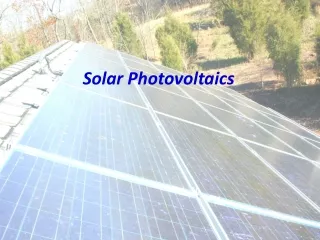
Solar electricity (photovoltaics) Teplin Airstrip, Germany: 130 MW on 2 km2 installed in 4 months Roof top installation (Kaneka a-Si modules) c.f. Centrale de GdDixence: 2 GW, 8 km2 lakes + catchment area Suitable roof top area in Switzerland: 138 km2 (residential, commercial, etc.) (IEA) F.-J. Haug – Photovoltaics
e e h h What is inside a solar cell? silicon wafer solar cell p-n junction thin film silicon solar cell p-i-n junction glass glass transparent front contact encapsulation p-layer n-contact semiconductor absorber layer p-type wafer n-layer reflecting back electrode metallic back contact encapsulation encapsulation glass glass F.-J. Haug – Photovoltaics
What is inside a solar cell? active part: semiconducting silicon (crystalline) active part: semiconducting silicon (thin film) (also used: CdTe, CIGS etc.) glass glass encapsulation n-contact 2-3 μm 200-300 μm encapsulation encapsulation glass glass F.-J. Haug – Photovoltaics
What is a semiconductor? • It’s conducting, but not as good as metals • Electric conductivity is normally associated with the flow of electrons in metals • Conductivity in semiconductors is different • The flow of water can serve as analogue F.-J. Haug – Photovoltaics
Conductivity in metals Analogue: a pond of water Flow of electrons similar to flow of water Horizontal surface, no (very small) potential difference F.-J. Haug – Photovoltaics
Electronic conductivity in a semiconductor Winter: the pond is covered with ice F.-J. Haug – Photovoltaics
Electronic conductivity in a semiconductor Winter: the pond is covered with ice Winter: the pond is covered with ice Flow of electrons similar to flow of water (like metals) Difference: Slower movement, needs potential difference F.-J. Haug – Photovoltaics
Hole conductivity in a semiconductor Imagine: blow air bubbles under the ice sheet Anew phenomenon, exclusive to semiconductors ! Bubbles under the barrier move upwards In semiconductors: positive charge carriers called holes F.-J. Haug – Photovoltaics
Why semiconductors for solar cells? e- h+ F.-J. Haug – Photovoltaics Metals normally reflect light; semiconductors can absorb it Absorbed light creates pairs of electrons and holes (water droplets above and bubbles below the ice sheet) An electric field between doped regions separates electron-hole pairs (imagine you inclined the ice sheet)
- - + + Absorption in semiconductors: bandgap Photons with energy less than the band gap are not absorbed Photon energy in excess of band gap is lost to thermalization High bandgap: high el. potential low current Low bandgap: low el. potential high current F.-J. Haug – Photovoltaics
Limiting efficiency Theoretical limit of ~33%, optimum bandgap 1.44 eV certified records: 28.8%: crystalline GaAs (Alta Devices) 25.6%: crystalline silicon (Panasonic) 20.5%: thin film Cu(In.Ga)Se2, (Solibro) F.-J. Haug – Photovoltaics
Better use of incident light: tandem cells high gap glue low gap Theoretical limit of ~43%, optimum bandgaps 1.1 and 1.7 eV certified records (triples): 37.9: crystalline (In,Ga)P/GaAs/(In,Ga)As (Sharp) 13.4%: thin film a-Si/nc-Si/nc-Si (LG) F.-J. Haug – Photovoltaics
Wafers or thin films? Thin film modules: size determined by glass and machinery e.g. thin film silicon tandem modules 5.3 m2(Applied Materials machinery) 1.4 m2(TEL Solar (ex Oerlikon) machinery) Crystalline cells: size determined by wafer e.g. c-Si: single-crystalline: max 30cm diameter multi-crystalline: typically cut to 15x15 cm2 high efficiency – high cost moderate efficiency – low cost F.-J. Haug – Photovoltaics
Wafers or thin films? Polycrystalline or amorphous materials: defects and grain boundaries recombination and short lifetime Crystalline material: perfect properties excellent lifetime and collection e- e- e- e- Electric field: Electric field: h+ h+ h+ h+ F.-J. Haug – Photovoltaics
Module interconnection SaFlex/TEL Solar SunPower Wafer based: solder cells into strings (e.g. SunPower: 22.4%) Thin film: 3 x laser scribing during process (e.g. TEL Solar: 12.2%) Rowell, En. Env. Sci F.-J. Haug – Photovoltaics
Thin film advantage Colorful TF-Si modules (PV-Lab prototypes) Semi-transparent a-Si modules (Schott) F.-J. Haug – Photovoltaics
Thin film advantage Roof tile laminate (Bressler) Flexible a-Si modules (Flexcell) • (UniSolar) F.-J. Haug – Photovoltaics
Thin film dilemma • PV modules are sold by power, currently: • ~0.8 $/W crystalline • ~0.6 $/W thin film 3.5$/W in 3.5 y Balance of System (BOS) “cost baseline” 3.5$/W in 3.5 y • PV system cost (currently ~5 $/W) • includes items that scale with area • (mount, wiring, labour, etc.) • For given power kWp, a larger area is needed, higher cost takes longer for amortisation F.-J. Haug – Photovoltaics
PV landscape in Switzerland PV-Lab systens inverters 3S Laminators MB wafer sawing Pasansun simulators Roth and Rau (CH) flexible CIGS Neuchâtel Equipment (end 2014) PV-Lab c-Si, TF-Si PV-Centre dye sensitized solar cells module testing dye cells F.-J. Haug – Photovoltaics
What we do at PV-Lab TF-Si challenge: weak absorberption especially for long wavelengths (red light) Solution: add back reflector => 2x absorption add texture for scattering => up to 50x Superstrate (glass) TCO p growth i n TCO back reflector p-i-n (usually on rigid glass) F.-J. Haug – Photovoltaics
Textured ZnO:Belectrodes • Requirements: • conductivity: add B-dopant (diborane) • surface texture for light scattering • Examples: ZnO:B (PV-Lab std.) SnO2:F (commercial, Asahi) W. Wenas, Jap. J. Appl. Phys (1991) S. Faÿ, EU PV Conf. (2000) F.-J. Haug – Photovoltaics
Take care with texturing! Collision of growth fronts on facets yields defective material ! Here: μc-Si, but also observed in a-Si H. Sakai, Jap. J. Appl. Phys. (1990) Y. Nasuno, Jap. J. Appl. Phys. (2001) M. Python, J. Non-Cryst. Sol., (2008) F.-J. Haug – Photovoltaics
Cells on flexible plastic substrate Nano-imprinting used for texturing of plastic (here: periodic grating structure) T. Söderström, Appl. Phys. Lett, (2009) K. Söderström, Prog. in PV, (2010) J. Escarré, J. Optics, (2012) R. Biron, Sol. En. Mat. (2013) F.-J. Haug – Photovoltaics
Heterojunction solar cells Surface passivation • c-Si is a perfect crystal; cell-performance is not bulk- but surface-limited • Intrinsic (undoped) a-Si:H provides excellent passivation of c-Si surface • Charge isextractedthroughpassivatinga-Si:H bi-layers • High efficiency cells >22% (certified) • A. Descoedre, EU-PV Conf., (2012) F.-J. Haug – Photovoltaics
Research on hetero-junction cells • Thin a-Si layers: max 5 nm • Pure a-Si layers: avoid epitaxy on underlying c-Si • Chemical annealing: alternate SiH4 and H2 plasma • Other: • Texture etch (avoid sharp valleys) • Highly transparent TCOs (very high transmission at 1100 nm) • Replace screen printing of Ag contacts by galvanic Cu F.-J. Haug – Photovoltaics
Thanks for your attention • Acknowledgementfor funding • SwissFederal Office for EnergyEU FP6 and FP7, CTI, FNS, CCEM-CH, SwissElectric Research, AxpoNaturstromfonds, Velux-Stiftung, IBM… • Bosch, OerlikonSolar, Pasan, Flexcell, Solvay, Dupont, Metalor,Meyer-Burger (3S Moduletec, Roth and Rau), Indeotec SA, … • Thanksalsoto the PV-Labmembers F.-J. Haug – Photovoltaics