Download
1 / 1
20 likes | 197 Vues
Silicon Photovoltaics. Nanophotonics. Introduction. Scattered.

E N D
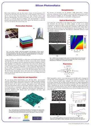
Silicon Photovoltaics Nanophotonics Introduction Scattered We envisage an increasing role for photonics within photovoltaics, avoiding reflectance, enhancing absorption lengths by increasing light-trapping and up and/or down conversion techniques are all increasingly important. In particular we see optical biomimetics and plasmonics as particularly exciting prospects. Photovoltaic technologies split into three distinct concepts, the first generation (1G) of devices has been based on wafer silicon, the second generation (2G) of devices will be based on thin film semiconductors on cheap substrates. Future, high efficiency third generation (3G) devices will make more use of the solar spectrum. Our aim is to develop deposition techniques and nanotechnologies to develop materialsand metamaterials that can be used to improve the efficiency or reduce the cost of 1G, 2G and 3G silicon-based solar cells. Incident Transmitted Absorbed Optical Biomimetics Over many tens of thousands of years nature has evolved nanostructured surfaces that efficiently deal with direct and diffuse sunlight. In order to be stealthy (transparent or antireflective (AR)), to stay cool (reflective) or to signal (black, white, iridescent). In addition to demonstrating these potentially useful optical effects, natural nanostructured surfaces are often hydrophobic and self-cleaning. The 2.5D or 3D structures observed in nature are often difficult to understand, difficult to model and difficult to fabricate. Scattered Photovoltaic Devices (b) (a) a-Si top cell amorphous Si:H a-SiGe middle cell amorphous SiGe:H (a) μc-SiGe bottom cell (c) Fig. 1. We aim to maintain state-of-art capability in the fabrication of first, second and third generation solar cells. This will involve (a) devices based on silicon wafers , (b) single-junction thin film silicon devices on flexible substrates and (c) emerging high-efficiency multi-junction thin film silicon solar cells (c) (b) Fig. 3. SEMs of (a) a transparent (AR) section of a hawk-moth and (b) biomimetic AR silicon (c) Detailed modelling of a nanostructured AR surface reveals complex dependence of reflectence on periodicity and shape. As part of a TSB project (EPISODE) in collaboration with Loughborough University and EcherKon Ltd. we will establish an in-house silicon wafer device capability (1G). We will use propriety deposition equipment provided by EcherKon to produce high throughput, low temperature epitaxial silicon that will provide efficient solar cells without the need for expensive wafers or large thermal budgets, thus providing a route to cheaper 1G devices. Meanwhile, as part of Supergen “Photovoltaics for the 21st Century” (EP/F029624) we will develop capability in silicon thin film device technologies based on amorphous-silicon (a-Si) and polycrystalline silicon (p-Si). We will develop “micromorph” devices (3G) made out of combined a-Si and p-Si junctions and develop high-efficiency triple-junction devices by adding SiGe layers to the tandem design. Plasmonics New materials and deposition Metal nanoparticles can have very strong interaction with light and by changing the size and shape of metal nanoparticles we can optimise structures to selectively absorb or scatter certain wavelength ranges. Inorganic solar cells are most likely to gain from strong scattering. We can produce metal nanoparticles by simply annealing thin metal films (fig3a) an thereby provide enhanced scattering in the 700 - 800nm range (fig3b). Alternatively we can use electron beam lithography o produce large pseudo-random arrays of bespoke particles (fig3c). We have found that Aluminium nanorods are found to produce strong scattering behaviour in the near bandgap region of a-Si solar cells (fig3.c) We can envisage future high-efficiency solar cells that utilize nanostructured materials. Semiconductor nanocrystals will be used to enhance absorption and tune band gap energies. Metal nanoparticles will help to scatter and trap light, and thin dielectric layers will be used to passivate semiconductor layers. Self-organised layers and nanostructures will be an increasingly important component of new solar cell designs and as a consequence, innovative deposition technologies will be of increasing importance. Our close collaborations with innovative manufacturers of deposition equipment (OPT, Plasma Quest and EcherKon) will allow rapid development of processes. (b) (a) (a) (b) Fig. 2. Self-organised and self-limiting deposition of monolayers and nanocrystals will be important within emerging solar cell designs (a) 4 layers of self-limited 3 monolayer thick Si3N4 (b) Germanium quantum dots grown in silicon by LPCVD. (c) (d) Fig. 3. (left) Raman scattering showing the G band of C-C bonds, the radial breathing mode (RBM) of carbon nanotubes, and the absence of the impurity D Contact: Prof Darren Bagnall, dmb@ecs.soton.ac.uk