Download
1 / 34
340 likes | 484 Vues
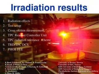
Irradiation results and Annealing scenarios for HPK. IEKP – University of Karlsruhe Alexander Furgeri Alex.furgeri@web.de. Outline. Overview of relevant sensor parameters Main results from p-irradiation prequalification W1TID-, IB1- and W3-Wafers for irradiation in Louvain

E N D
Irradiation resultsand Annealing scenarios for HPK IEKP – University of Karlsruhe Alexander Furgeri Alex.furgeri@web.de General Tracker meeting
Outline • Overview of relevant sensor parameters • Main results from p-irradiation • prequalification W1TID-, IB1- and W3-Wafers for irradiation in Louvain • Results from irradiation in Louvain • Scenarios of Udep for inner Barrel sensors • Conclusions General Tracker meeting
Parameters of sensors Resistivity: expected to be <2kΩcm> varying from 1.25 to 3.25kΩcm Full depletion voltage: Effect of thickness: 320µm 290µm (30µm n+-layer) ~19% less depletion voltage ! Higher resistivity lower depletion voltage For allowed range of resistivity: 130V < Udep <350V General Tracker meeting
Differences diodessensors The depletion voltage for sensors are also depending from geometrie factors. The lowest is : ~1.16 (IB1) The highest is : ~1.31 (W3) Only HPK! General Tracker meeting
Changes of Rpoly after irrad + 0.35 MΩ + 0.15 MΩ HPK with high fluence ST with low fluence n-doped poly-Si Increase of Rpoly due to donor removal General Tracker meeting
Changes of CC after irrad For minis ~ -1pF, Difficult to see due to fluctuations of measurements with 100Hz. - 15pF HPK –sensor with high fluence General Tracker meeting
Results from proton irradiation • Small increase of Rpoly • small decrease of CaC • small increase of Cint • (for allowed flatband voltage range! • Defined from studies in KA) • Rint above limit • (introduced measurement signal below noise) • NO PINHOLES !!! • NO LEAKY STRIPS ! General Tracker meeting
Development of Udep Changes of Neff: • short term annealing • stable Damage • long term reverse annealing General Tracker meeting
Experimental data for donor removal in Hamburg model Results from KA p-irradiation rC <1 ! rC=NC,0/Neff,0 Describes complete or partial donor removal HPK with high fluence General Tracker meeting
Special n-irradiation (high res.) • Irradiation in Louvain of IB1,W3 & W1TID • Check for resistivity profile across wafer, (before irradiation) • Check if sensors follow the Hamburg model ! • Adjusting parameters and taking into account for scenarios • Check of new measurement methods of Louvain (Rpoly!) and cross check with Karlsruhe General Tracker meeting
Resistivity explained by HPK HPK delivered sensors with to high resistivity. Explanation from HPK: Wafers have a large variation of resistivity across wafer profile! But also sensors with a resistivity of >5kΩcm (70V) appeared in the community. Question: where does the depletion voltage end? General Tracker meeting
Prequalification W1TID • Diodes 2-5 and 10-13 • not measurable • breakdown for diodes • between 460V and 530V • depletion voltage for • diodes: 50V (for all !) • depletion voltage for • minis: 80V (~1.3*Udep of • diodes ?!) • Depletion voltage for • sensor 105V (profile of • HPK seems to be right) • Same profile for W3 General Tracker meeting
Irradiation in Louvain Only diodes choosen for adjusting the hamburg model! Reason: variation in correction Factors diodes↔Sensors due to resistivity profile! rc~ 0,3 (0.65) gc~ 1,2e-2 (1.49e-2) General Tracker meeting
Irradiation in Louvain Check if minisensors follow the Hamburg Model with the new exp. data! General Tracker meeting
Irradiation in Louvain Check if sensors follow the Hamburg model! gc~1.1e-2? rc~0.3 ! General Tracker meeting
Cross check Louvain KA Very good agreement for minisensors ! For sensors discrepances in Cint and CC! General Tracker meeting
Batches with high resistivity • HPK delivers sensors with high resistivity • higher depletion voltage in the end of CMS expected • Luminosity in the tracker • 1. year 10% • 2. year 33% • 3. year 67% • 4.-10. year 100% • Sensor fluence in reality depending from the location in the tracker • Radial location (especially for charged Hadron fluence) • Z-location (especially for neutron fluence in the endcaps) General Tracker meeting
Fluence distribution in the tracker Low variation in fluence for most geometries. Uncertanties in fluences: 50% General Tracker meeting
Calculation of the scenario • Local Distribution of fluence in the Tracker • Tracker-TDR • comparison with E. Migliore (same source ?!) • Fluences for different geometries • Per year: • Irradiation (at once) • Beneficial annealing (10°C & 20°C) • Reverse annealing (10°C & 20°C) • Scenario for 10 years • time without beam and annealing not shown General Tracker meeting
Time constants for HH For +20°C: τA=2.3 days τy=475 days For +10°C: τA=10 days τy=2920 days For –10°C: no significant change for 10 years To avoid reverse annealing keep temperature as low as possible! General Tracker meeting
A. Furgeri 28 days per year @ 20°C 5 Times higher time constant for beneficial annealing Donor removal (rC) from experimental data in Karlsruhe and Louvain (better for low resistivities, less uncertainties) gc from exp. data Geom. factors for sensors, confirm with exp. Data Factor of 1.5 for fluences E. Migliore 28 days per year @ 10°C 26 times reduced time constant for reverse annealing Complete donor removal for hadron fluences (worse for low resistivity, but not confirm with exp. data) gc from literature No correction factor (diodes instead of sensors) No factor for uncertainties in fluences Differences A. Furgeri E. Migliore General Tracker meeting
What‘s the allowed maximum for depletion voltage? • Max. 600V from power supplies • Factor of 1.5 for over depletion needed • Maximum for depletion voltage of 400V ?! Let‘s look where we are ! General Tracker meeting
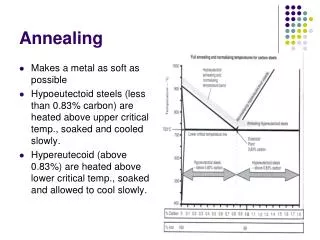
Description for following plots Before type inversion After type inversion Real scenario General Tracker meeting
Scenarios IB1 – 1. Layer Worst case for IB1, thickness 320µm, Annealing @20°C 14 days, Maximum 440V With actual thickness of 290µm: 360V Remember Udep~ d² Effect of higher resistivity: ~30V General Tracker meeting
Scenarios IB1 – 1. Layer Worst case for IB1, with thickness 320µm, 28 days @20°C per year Maximum 530V With actual thickness of 290µm: 435V General Tracker meeting
Scenarios IB1 – 1.Layer Worst case for IB1, with thickness 320µm, 28 days @ 10°C per year d= 290µm 320V General Tracker meeting
Scenarios W1 TEC & TID 14 days @ 20°C Maximum 400V 28 days @ 20°C Maximum 470V d= 290µm 320V d= 290µm 380V General Tracker meeting
Scenarios IB1 – 2.Layer 14 days @ 20°C Maximum 290V 28 days @ 20°C Maximum 330V General Tracker meeting
Scenarios W2 28 days @ 20°C Maximum 390V 14 days @ 20°C Maximum 320V d= 290µm 315V General Tracker meeting
Sceanrios W3 14 days @ 20°C Maximum 290V 28 days @ 20°C Maximum 350V d= 290µm 250V General Tracker meeting
Different donor removalin worst case scenario Effect of 40V for high res. 100v for low res. Donor removal of 65% for ch. Hadrons and 30% for neutrons, due to exp. data Complete donor removal for ch. Hadrons and 65% for neutrons Not confirm with exp. data General Tracker meeting
DiscrepancesIQC and Scenarios Effect of reverse annealing ~200V! Scenario for IB1- 1.Layer Result after IQC (no exp. data!) No reverse annealing! General Tracker meeting
Summary of uncertainties • Donor removal ? Irradiation in Lubljana in progress (9 minis) for different fluences. (higher statistic) • Temperature during shutdown and repair periods ? • CONDITIONS CONTROLLED ?! • Avoid reverse annealing ! Try to keep temperature below 20°C ! max. of +10°C for 4 weeks?! • Time of shutdown and repair periods ? • Open (warm up) the Tracker as late as possible ! • Fluences in different running periods ? • Effectiv thickness of sensors ? Changes in production? • … Ask me again after 10 years! General Tracker meeting
Conclusions • Worst case for IB1,(W1TEC & W1TID?) needs ~700V bias voltage, but expected to be better • Separation of sensors with different resistivities possible for IB1 (1. & 2. Layer) • No separation possible for W1 and W1TID • IB2,W2,W3 & W4 not critical (high res. accepted) • Question of high resistivity: Sensors accepted, with compromise, that the next sensors of IB1 will have a lower resistivity (1.25-2 kOhmcm) General Tracker meeting