THERMAL OXIDATION - Chapter 6
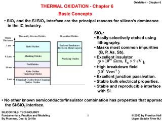
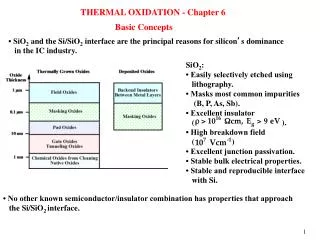
THERMAL OXIDATION - Chapter 6. Basic Concepts. • SiO 2 and the Si/SiO 2 interface are the principal reasons for silicon ’ s dominance in the IC industry. SiO 2 : • Easily selectively etched using lithography. • Masks most common impurities (B, P, As, Sb).

THERMAL OXIDATION - Chapter 6
E N D
Presentation Transcript
THERMAL OXIDATION - Chapter 6 Basic Concepts • SiO2 and the Si/SiO2 interface are the principal reasons for silicon’s dominance in the IC industry. • SiO2: • • Easily selectively etched using • lithography. • • Masks most common impurities • (B, P, As, Sb). • • Excellent insulator • ( ). • • High breakdown field • ( ) • • Excellent junction passivation. • • Stable bulk electrical properties. • • Stable and reproducible interface • with Si. • No other known semiconductor/insulator combination has properties that approach the Si/SiO2 interface.
Thermal Oxidation and SiO2 Interface Applications SiO2 grows on Si (also @ RT); enables very easy IC formation; ensures stability and reliability. Lower thermal budget 1 – 2 nm New dielectrics to avoid tunneling. (high K) Low K dielectrics
Historical Development and Basic Concepts Oxide growth using O16 and O18 isotopes identifies the mechanism. Neutral O2 and H2O and/or OH are dominant species in oxidation, not atoms or ions O, O- , O2-, Volume of SiO2 is 30% larger than Si. (1.3)3 ~ 2.2 volume of the oxide cannot be accommodated in Silicon • Oxidation involves a volume expansion (≈ 2.2X). • Especially in 2D and 3D structures, stress effects play a dominant role.
Silicon Consumption During Oxidation (LOCOS) Bird’s Beak formation Stress at the Si/Si3N4 interface
Structure of Silica Glass Short range order maintained Amorphous material hydrogen Non-bridging oxygen in fused Silica (not present in crystalline SiO2) Network modifier ----> Qm Si can be replaced by deposits. B,P,As or Sb = network formers. • large compressive stress (5*109 dynes/cm2) exists in SiO2. High temperature can relief stress by viscous flow. • Large difference in the thermal expansion coefficients of Si and SiO2. Silicon in tension refer to curvature
• SiO2 is amorphous even though it grows on a crystalline substrate. (Intel Web site) • Four charges are associated with insulators and insulator/semiconductor interfaces. • Qf - fixed oxide charge • Qit - interface trapped charge • Qm - mobile oxide charge • Qot - oxide trapped charge
SiO2/Si System: Structure and Charges (Fig 3.15) amorphous/crystalline – interface flat. (TEM) Roughness with growth rate and T. Detect density at the interfaces is ~ 109 – 1011 cm-2. Trapped charges Qot important when isolation radiation is present (space applications, plasma processing) EPROM Fixed charge ~ 109 – 1011 cm-2 is + and does not change in device operation. Interface charge =traps due to dangling Si bonds change in operation QpQit – both related to unoxidized Si atoms. Deal triangle Reduce charges since they degrade device operation T , H2 anneal..
Oxide Charges and Their Annealing H fast through SiO2 Al annealing: Al+OH ”ALO”+H “t” to reach equilibrium with T Qit H2 2H Si•+HSiH Increasing surface roughness increases charges (100) Si used in ICs Ar better - does not react with Si.
• Oxidation systems are conceptually very simple. • In practice today, vertical furnaces, RTO systems and fast ramp furnaces all find use. LOCOS or STI Gate Oxides DRAM Dielectrics • Thermal oxidation can potentially be used in many places in chip fabrication. In practice, deposited SiO2 layers are increasingly being used (lower Dt).
Manufacturing Methods and Equipment Vertical furnaces are also used. Better uniformity, easier automation, cleaner - no contact with the tube Wafer loading should use cantilever or elavators (perpendicular) to avoid touching the walls. 3 zones + 0.5 ° C Dry or wet oxidation Ramping of T from/to 800 °C ( 10 °C/sec) Add HCl or TCA for gettering purpose (metals, Na +) @ 1000 °C, in water, 2X for each 100 °C Temperature control + 0.5 °C
Measurement Methods • Physical (Destructive) : Etch a step and measure (stylus, microscope with monochromatic light, • AFM, SEM, TEM) • Optical (usually non destructive): thick oxides (color chart, ellipsometry, reflectance) but for thin oxides: ellipsometry REFLECTANCE white or monochromatic light Refraction indexes Color chart (xox > 50nm) –> not destructive interference will affect the reflected light –> color correlated with thickness of a dielectric layer (10-20 nm accuracy) - use standards For monochromatic light minima and maxima in the reflected beam allow to determine xox (fringes, spectrometers with sweeping wavelength l for fixed we can find extrema) Good for a few tens of nm Ellipsometry uses polarized light and detect the change in polarization of the reflected light due to a film (thickness, index of refraction) 1,2,3 max 1/2… min
• Powerful technique for characterizing semiconductor/ insulator structures. Electrical Measurements C-V Measurements MOS Capacitor accumulation Capacitance-voltage method ac signal xox obtained Charge Density depletion Inversion Equilibrium conditions. Nd obtained
CV Measurements Low frequency (~1Hz), high frequency (100Khz – 11) AC signals used for C-V Measurements.) QI follows QG C =COX XD= XDmaxQD fixed * XD> XDmax Holes generated in the D.L and attracted by the gate source the DL when |VG| increases High frequency AC signal changes faster than QI can respond (generation is slow) To avoid deep depletion*:
Charges Derived Qm, Qot have similar effect as Qf (shift characteristics) P-type Due to traps EitEc States near Ec Qi present Eit Ev Midgap states Traps cannot charge or discharge - do not respond to HF signal States near Ev Always present Qi respond to DC voltage – stretch out change in EF (VG), charges at Eit. Stress of the oxide (ex. charge injection, radiation) C-V degradation ( time to breakdown, charge to breakdown)
Experiment : Why no C-V change is observed? • Assume good oxide/Si interface. • Masking oxide was too thin high doping under the gate (CD) • Supply of carriers would give, C-VHF = C- VLF
Models and Simulation First -Order Planar Growth Kinetics - Linear Parabolic Model Boundary layer In steady state F1=F2=F3 Deal and Groove Model Reaction at Si surface Henry law C*≈CO (PG≈PS) Oxidant solubility in SiO2 h hG- mass transfer coefficient Gradient CoCi h=hG/HkT Transport of the oxidant to the oxide surface. Transport to Si = Diffusion of O2 (H2O) through the oxide Sol.sol. in SiO2 ksx0/D <<1 or ksx0/D >>1
Models and Simulation First Order Planar Growth Kinetics – Linear Parabolic Model transport reaction ksx0/D <<1 CI C* Diffusion fast compared to chemical reaction for thin oxides. ksx0/D >>1 Fast reaction - diffusion limits oxidation (thick oxides) Fitting parameters CI0 xo(t) General dependence of oxide thickness on time. ks&D=f(t) Transition region @about 50-200 nm Linear rate constant parabolic Rate constant Thin oxides Thick oxides
Linear and Parabolic Rate Constants Experimental results Derivation of A & B Arrhenius dependence Parabolic Linear Represent Si-Si bond breaking activation energies E2 Linear Parabolic * Breaking Si bonds diffusion parabolic * E1 Represent diffusion of O2 or steam Bwet>Bdry because Cwet* >> Cdry* @1100 °C, 3*1019 cm-3 >> 5*1016 cm-3 !!
Wet oxidation - used for thicker oxides Dry oxidation - used up to 100-200 nm C*|wet>>C*|dry c) a) b) Calculated (100) silicon dry O2 oxidation rates using Deal Grove. Calculated (100) silicon H2O oxidation rates using Deal Grove. Example: Problem 6.13 in the text: a) 3 hrs in O2 @ 1100 ˚C = 0.21 µm + b) 2 hrs in H2O @ 900 ˚C = 0.4 µm + c) 2 hrs in O2 @ 1200 ˚C = 0.5 µm total oxide thickness.
Thin Oxide Growth Kinetics • A major problem with the Deal Grove model was recognized when it was first proposed - it does not correctly model thin O2 growth kinetics. • Experimentally O2 oxides grow much faster for ≈ 20 nm than Deal Grove predicts. • MANY models have been suggested in the literature. 1. Reisman et. al. Model (17) • Power law “fits the data” for all oxide thicknesses. • a and b are experimentally extracted parameters. • Physically - interface reaction controlled, volume expansion and viscous flow of SiO2 control growth. 2. Han and Helms Model (18) • Second parallel reaction added - “fits the data”” for all oxide thicknesses. • Three parameters (one of the A values is 0). • Second process may be outdiffusion of OV and reaction at the gas/SiO2 interface.
3. Massoud et. al. Model (19) • Second term added to Deal Grove model - higher dx/dt during initial growth. • L ≈ 7 nm, second term disappears for thicker oxides. • Easy to implement along with the DG model, used in process simulators. • Data agrees with the Reisman, Han and Massoud models. (800˚C dry O2 model comparison below.)
Other Models for Planar Oxidation Kinetics -> Incorporate Thin Oxides linear D-G model fails For thin oxides< 20nm • Models: • O2- coupled diffusion with holes • thermionic emission of e- from Si • micropores, channels - parallel transport • parallel oxidation with O2, O (diffusion and reaction) • silicon surface with additional sites 800 °C Volume expansion at the interface provided by viscous flow - model applicable to 2D oxidation in nonplanar structures a,b=f(T, p.press.) 1) 2) O2 through SiO2, O2+ O @Si =parallel reactions O dominates @low T O2 dominates @ high T 1000°C 3) B/A a Pn n=1 H2O, n=.5 Dry O2 4) Massoud et al. L=7nm Good for thin oxides Added for thin oxides
Effect of Volume Mismatch in Si/SiO2 System; Recessed LOCOS H2O@1000°C; Find time to get planar surface? Example: 2.2X volume expansion -> 45%yox=ySi so yox=ySi/.45 ySi Total oxide thickness to be grown: yox=ySi/0.45=ySi+0.5µm ySi=0.41µm yox=0.91µm For H2O Time for dry oxidation would be unrealistically long
Dependence of Growth Kinetics on Pressure Dry O2 if C*aPG B, B/A PG dxo/dt PG 0.1 atm D-G model gives good match for wet oxidation not for dry - linear-parabolic model is incomplete BP B/APn 0.5<n<1.0 Many models use modified Si/SiO2 interface reaction - none is widely accepted 10 atm D-G model with correction: B/A=(B/A)iP B=(B)iP for H2O) B/A=(B/A)iPn B=(B)iP for O2 n≈0.7-0.8
Mixed Ambient Growth Kinetics Role of Cl in Oxidation Processes Mixed ambient B/A B f(HCl) • Two terms include independent reactions for • *H2O and O2 (not a good model) • *H2O/HCl (first term only) and • *O2/HCl interaction between oxidants - dependence -> pressure role
Orientation Effects in Oxidation wet dry (100), (111), and Polysilicon Density of atoms (bonds) in (111)>(100) No effect of orientation in the parabolic regime Very thin oxide growth at high pressure and low T (ex. 800°C): (100) >(111) In the linear regime Related to stress Simulated oxide growth
C. 2D SiO2 Growth Kinetics • These effects were investigated in detail experimentally by Kao et. al. about 15 years ago. • Typical experimental results below. (Kao et.al)
2D SiO2 Growth Kinetics Difference in volume -> problems when expansion is restricted (SiO2 confined) • Experiments by Kao et al.: • Retardation at sharp corners (2X for 500 nm SiO2) • Retardation larger @ low T (no effect @ 1200 °C) • Interior (concave) corners oxidize slower than exterior (convex) but both slower than flat Si • Reasons • Crystal orientation • Diffusion of oxidant through amorphous SiO2 is the same -> no dependence on direction • Stress (volume difference): SiO2 under large compressive stress -> affect both oxidant transport and reaction at the Si surface Poly-Si for contrast
•In addition, the flow properties of the SiO2 need to be described by a stress dependent viscosity (23) Where is the shear stress in the oxide and VC is a fitting parameter. SUPREME uses many fitting parameters. • These models have been implemented in modern process simulators and allow them to predict shapes and stress levels for VLSI structures (above right). • ATHENA simulation: Left - no stress dependent parameters, Right - including stress dependence.
Oxidation of Non-Planar Structures Example Stress retards oxidation; @high T viscoelastic flow relaxes stress Oxide viscosity=f(stress, T) Stress @T> Stress @T no stress Stress included (outer) Reaction diffusion solubility (inner) Viscoelastic properties (nonlinear in T) of poly-Si, Si3N4 also have to be included in simulations of oxidation History of Stress VERY IMPORTANT Stress in an oxide depends on growth T. In sequential processing, transient will appear in the next step @ higher T from the original stress (=higher at lower T) which sets the oxide growth rate below that at high T (lower stress). stress dependent activation values Also TF(irst)>TS(econd) StressF<StressS GrowthF>GrowthEquilibrium • Relieve stress: • High T - not good for ICs • O2/NF3 ? • Corona discharge ?
Segregation of Dopants at the Si/SiO2 Interface B B in H2 Dry O2 Ga - not useful as a dopant P, As
Point Defect Based Models • The oxidation models we have considered to this point are macroscopic models (diffusion coefficients, chemical reactions etc.). • There is also an atomistic picture of oxidation that has emerged in recent years. • Most of these ideas are driven by the volume expansion occurring during oxidation and the need for “free volume”. • In Chapter 3 we described internal oxidation in the following way: Oxidation Enhanced Diffusion (OED) Oxidation Retarded Diffusion (ORD) Both are related to the interface reaction (B/A or ks) Si/SiO2 - generation of I ~ 1/103 Si atoms diffuse to Si, others oxidized • Surface oxidation can be thought of in the same way.
• The connection between oxidation and other processes can then be modeled as shown below. Increase in concentration of Si-I -> OED also laterally ATHENA simulation of OED. Original B layer was uniform • Oxidation injects interstitials to create “free volume” for the oxidation process. • Oxidation can also consume vacancies for the same reason. • These processes increase I concentrations and decrease V concentrations in nearby silicon regions. • Any process (diffusion etc) which occurs via I and V will be affected.
Advanced Point Defects Based Model for Oxidation Relation to dopant diffusion Interstitials (I) diffuse far G-R determine a net flux of I -> effect on diffusion even in a buried layer. • Experimental G-R for various layers (both depend on surface layer) • Reasons: • kinks on the surface; • generation/surface • regrowth/segregation/Si/SiO2
Substrate Doping Effects Concentration Enhanced Oxidation (CEO) 5x faster due to dopant 2x faster NDopant P -> oxide growth by B/A not by B; especially @ low T about 3-4X due to concentrations Properties of oxide do not change for P but change for B Low T High T Oxidation needs V for volume expansion so for dopant concentrations, charged V (V-, V= - N+-type; V+ - P+ -type) -> B/A Dopant segregation N+ -> to Si P+ -> SiO2 Interface changes during oxidation -> growth rate changes CEO stronger for N+ than P+ (B/A grows, B does not) CEO for Boron changes B but not B/A due to incorporation in the oxide
Complete Process Simulation of Oxidation • Many of these models (and others in Chapter 6), have been implemented in programs like SUPREM. • Simulation of an advanced isolation structure (the SWAMI process originally developed by Hewlett-Packard), using SSUPREM IV. The structure prior to oxidation is on the top left. A 450 min H2O oxidation at 1000 ˚C is then performed which results in the structure on the top right. An experimental structure fabricated with a similar process flow is shown on the bottom right. The stress levels in the growing SiO2 are shown at the end of the oxidation on the bottom left.
Silicide Oxidation - Similar to Silicon Silicides (TiSi2, CoSi2) used in ICs instead of polysilicon (400 µΩcm) local interconnects Oxidation results in formation of SiO2 (for most metals) or mostly MOx for HfSi2, ZrSi2, TiSi2 Metal bonds break -> M diffuses to the Si (polysilicon) substrate, released Si form SiO2 For TiSi2 Si atoms diffuse from the poly_Si For CoSi2, NiSi2, PtSi - metals diffuse to poly_Si Bsilicide = Bsilicon B/Asilicide>>B/Asilicon Parabolic growth
Polysilicon Oxidation Rate larger than (100) because of various orientations and sizes of grains -> B/A=f(grain size) not B Grain boundary important in doping, regrowth at high T Si3N4 Growth and Oxidation Kinetics Niride is a mask against in LOCOS Si3N4 growth slow in NH3 2.5-7.5 nm @900°C or Si2N2O Kooi effect Small diffusion of oxidants through Si3N4
Oxidation Induced Stacking Faults (Preferential Etching) OISF with time and temperature of the oxidation process Preferential etching reveals S-pits and OISF Surface and bulk OISF Increasing etching time
Formation and Annihilation of OISF in Wet and Dry Oxidation Processes OISF depend on available I at the Si surface Wet Dry Oxidation
Summary of Key Ideas • Thermal oxidation has been a key element of silicon technology since its inception. • Thermally, chemically, mechanically and electrically stable SiO2 layers on silicon distinguish silicon from other possible semiconductors. • The basic growth kinetics of SiO2 on silicon are controlled by oxidant diffusion and Si/SiO2 interface chemical reaction. • This simple Deal-Grove model has been extended to include 2D effects, high dopant concentrations, mixed ambients and thin oxides. • Oxidation can also have long range effects on dopant diffusion (OED or ORD) which are modeled through point defect interactions. • Process simulators today include all these physical effects (and more) and are quite powerful in predicting oxidation geometry and properties.