Chapter 6 OXIDATION
Chapter 6 OXIDATION. Professor Masoud Agah ECE Department. Introduction. Si is unique in that its surface can be passivated with an oxide layer layers are easily grown thermally Layers can be deposited

Chapter 6 OXIDATION
E N D
Presentation Transcript
Chapter 6OXIDATION Professor Masoud Agah ECE Department
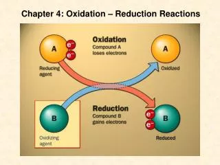
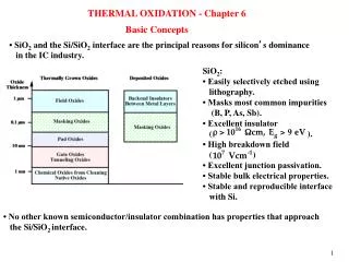
Introduction • Si is unique in that its surface can be passivated with an oxide layer • layers are easily grown thermally • Layers can be deposited • The Si/SiO interface is the most carefully studied interface in all of science/engineering • it has few defects • It is stable over time • Its mechanical and electrical properties are almost ideal • they adhere well • They block diffusion of dopants • They are resistant to most chemicals used in the process • They can easily be patterned and etched with specific chemicals or dry etched with plasmas
Introduction • Thermal oxide properties: • Amorphous (why?) • Density: 2.27g/cm3 • Dielectric constant: 3.9 • DC resistivity @ 25C: 1016-cm • Energy gap: 9eV • Thermal conductivity: 1.3W/mC • Refractive index: 1.46 • Melting point: 1700C • Molecular weight: 60.08 • Molecules: 2.3x10²²/cm3 • Specific heat: 1J/gC • Film stress: Compressive 0.2-0.4GPa • Etch rate: BHF 100nm/min
Introduction • MOS structures are easy to build and devices are reliable and stable • Oxide is used for several applications • Gate dielectric • Mask against ion implantation or diffusion • For isolation of various lateral regions • As insulator between various metal layers
Introduction • Key oxide issues are summarized by the NTRS in the following table • Note that most of the issues deal with very thin gate oxides (< 10 nm) • The last two rows in the table deal with thicker oxides used for masking and back end processing
Introduction • Si will oxidize at room temperature to form a layer 0.5 - 1 nm (5- 10 Å) thick very quickly • The reactions slows and stops with layers 1 – 2 nm thick after a few hours • The oxide depends on the surface treatment and structure
Introduction • The most critical application is the gate oxide • These layers are now 3 – 5 nm thick (25-50 atomic layers thick) • They are projected to be < 1 nm in a few years • It is remarkable that we can build layers like this in the tens of millions per device and they all work (are defect-free) and will sustain about 50% of the theoretical breakdown voltage of the bulk material (10 – 15 MV/cm) • Their thicknesses must be controlled to about the level of 1 atomic layer
Introduction • It is going to be harder and harder to control these structures • Oxynitride films are likely to be part of the solution • When films get this thin, we have to deal with QM tunneling (i.e., the finite probability the and electron can pass trough a barrier that is higher than its energy) • Tunneling is usually undesirable, but some devices are now built using this phenomenon (nonvolatile memory)
Introduction • We need to recall that we can deposit oxide and oxynitride layers via CVD or LPCVD • This is essential for those parts of the process where we have covered all the Si and there is no path for Si from the wafer to the oxidizing interface • Deposited layers are usually thicker than thermal layers because we cannot control the thickness as well • If we properly anneal deposited layers, we can get electrical properties that are almost as good as those of thermally gown oxide layers
Basic Concepts • It has been demonstrated several times over the past 30 years that the oxide grows by diffusion of oxygen/H2O through the oxide to the Si/SiO2 interface • Thus, a new interface is continuously growing and moving into the Si
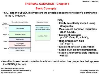
Basic Concepts • The process involves an expansion since the density of an equal volume of Si occupies less space than a volume of oxide containing the same number of Si atoms • Nominally, the oxide would like to expand by 30% in all directions; but it cannot expand sideways because it is constrained by the Si atoms • Thus, there is a 2.2 expansion in the vertical direction • In figure 6-4, note the growth of the LOCOS oxide above the surface • Also note the “bird’s beak” of oxide under the nitride layer
Basic Concepts • If there are shaped surfaces where oxide must grow, this expansion may not be so easily accommodated • The oxide layers are amorphous (i.e., there is only short range order among the atoms) • There are no crystallographic forms of SiO2 that match the Si lattice • The time required for transformation to a crystalline form at device temperatures is very very long
Basic Concepts • The oxide that grows is in compressive stress • This stress can be relieved at temperatures above 1000C by viscous flow • There is a large difference in the TCE between Si and SiO2 • The increases the compressive stresses in the oxide and results in tensile stresses in the Si near its surface • The Si is very thick while the oxide is very thin; the Si can usually sustain the stress • Since the wafer oxidizes on both sides, the wafer remains flat; if you remove the oxide from the back side, you will see a warping of the wafer • The stress can be measured by measuring the warp of the wafer
Basic Concepts • The electrical properties of the Si/SiO2 interface have been extensively studied • To first order, the interface is perfect • The densities of defects are 109 – 1011 /cm2 as compared to Si atom density of 1015 /cm2 • Most defects are associated with incompletely oxidized Si • Deal (1980) suggested a nomenclature that is now used to describe the various defects (Read it in the textbook)
Defect Nomenclature (read in textbook) • There are four type of defects • Qf is the fixed oxide charge. • It is very close (< 2 nm) to the Si/SiO2 interface • It is about 109 –1011/cm2 • It is related to the transition from Si to SiO2 • It is positive and does not change with under normal conditions
Defect Nomenclature (read in textbook) • Qit is the interface trapped charge • It appears to be due to incompletely oxidized Si • It is very close to the interface • It may be positive, neutral, or negative • It’s charge may change during device operation due to the trapping of electrons or holes • Energy levels associated with these traps are distributed throughout the forbidden band, but there seem to be more near the valence and conductions bands • The density of traps is 109—1011 cm-2 eV-1 (about the same as for Qf)
Defect Nomenclature (read in textbook) • Qm is the mobile oxide charge • It is not so important today but was very serious in the 1960’s • It results from mobile Na+ and K+ in the oxide • The shift in VTH is inversely proportional to COX and thus, as oxides become thinner, we can tolerate more impurity
Defect Nomenclature (read in textbook) • Qot is charge trapped anywhere in the oxide • These seem to be related to broken Si-O bonds in the bulk oxide (well away from the interface) • The bonds may be broken by ionizing radiation or by some processing steps such as plasma etching or ion implantation • They are normally repaired by a high-temperature anneal • They can trap electrons or holes • This is becoming more important as the electric field in the gate oxide is increased • They result in shifts in VTH
Defect Nomenclature (read in textbook) • All four types of defects have deleterious effects on the operation of devices • High temperature anneals in Ar or N2 near the end of process flow plus an anneal in H2 or forming gas at the end of process flow are used to reduce their effect
Manufacturing Methods • Oxidation systems are among the simplest of semiconductor processing equipment • They require • An oven capable of 600 – 1200 C with a uniform zone large enough to hold several wafers • A gas distribution system to provide O2 and H2 • A control system that holds the temperatures and gas flows to tight tolerances (0.5 C)
PRODUCTION FURNACES • Commercial furnace showing the furnace with wafers (left) and gas control system (right).
PRODUCTION FURNACES • Close-up of furnace with wafers.
Models • The first major model is that of Deal and Grove (1965) • This lead to the linear/parabolic model • Note that this model cannot explain • the effect of oxidation of the diffusion rate • the oxidation of shaped surfaces • the oxidation of very thin oxides in mixed ambients • The model is an excellent starting place for the other more complicated models
CHEMICAL REACTIONS • Native SiO2 produced on surface is a high quality insulator and good diffusion barrier • Process for dry oxygen Si + O2 SiO2 • Process for water vapor Si + 2H2O SiO2 + 2H2
OXIDE GROWTH • Si is consumed as oxide grows and oxide expands. The Si surface moves into the wafer. Original surface 0.54 Xox SiO2 0.46 Xox Silicon wafer
MODEL OF OXIDATION • Oxygen must reach silicon interface • Simple model assumes O diffuses through SiO2 • Assume no O accumulation in SiO2 • Assume the rate of arrival of H2O or O2 at the oxide surface is so fast that it can be ignored
No Silicon dioxide J Silicon N Ni SiO2 Si Xo Distance from surface, x Deal-Grove Model of Oxidation • Fick’s First Law of diffusion states that the particle flow per unit area, J (particle flux), is directly proportional to the concentration gradient of the particle. • We assume that oxygen flux passing through the oxide is constant everywhere.
Deal-Grove Model of Oxidation • Assume the oxidation rate at Si-SiO2 interface is proportional to the O concentration: • The growth rate is given by the oxidizing flux divided by the number of molecules M of the oxidizing species that are incorporated into a unit volume of the resulting oxide:
Deal-Grove Model of Oxidation • The boundary condition is • The solution of differential equation is
Deal-Grove Model of Oxidation xox : final oxide thickness xi : initial oxide thickness B/A: linear rate constant B : parabolic rate constant • There are two limiting cases: • Very long oxidation times, t >> • xox2 = B t • Oxide growth in this parabolic regime is diffusion controlled. • Very short oxidation times, (t + ) << A2/4B • xox= B/A ( t + ) • Oxide growth in this linear regime is reaction-rate limited.
Temperature (0C) 1200 1100 1000 900 800 700 10.0 1.0 H2O (640 torr) EA = 2.05 eV 0.1 B/A (mm/hr) (111) Si (100) Si 0.01 Dry O2 EA = 2.0 eV 0.001 0.0001 0.6 0.8 0.9 1.0 0.7 1.1 1000/T (K-1) Deal-Grove Model of Oxidation • At short time • B/A is the linear rate constant • Process is controlled by the reaction at the Si surface
Temperature (0C) 1200 900 800 1100 1000 1.0 H2O (640 torr) EA=0.78eV 0.1 B(mm2/hr) 0.01 Dry O2 EA=1.23eV 0.001 1.0 0.6 0.7 0.8 0.9 1000/T(K-1) Deal-Grove Model of Oxidation • At long time • B is the parabolic rate constant • Process is controlled by diffusion of O through oxide
B P 1200 C Mask thickness (mm) 1200 C 1100 C 1100 C 1000 C 900 C 1000 C 900 C Diffusion time (hr) Oxide as a Diffusion Barrier • Diffusion of As, B, P, and Sb are orders of magnitude less in oxide than in silicon • Oxide is excellent mask for high-temperature diffusion of impurities 10 Boron Phosphorus 1 0.1 0.01 0.1 1.0 10 100
Deal-Grove Model Predictions • Once B and B/A are determined, we can predict the thickness of the oxide versus time
Other Models • A variety of other models have been suggested, primarily to correct the deficiencies of the Deal-Grove model for thin oxides • These include • The Reisman power law model • The Han and Helms model with parallel oxidation paths • The Ghez and van Meulen model to account for the effect of oxygen pressure • Some of these models do a much better job for thin oxides • None are widely accepted
Other Topics • Several topics other than the simple planar growth of wet and dry oxide are important • These include • Thin oxide growth kinetics • Dependence on oxygen pressure • Dependence on crystal orientation • Mixed ambient growth kinetics • 2D growth kinetics • These topics are covered well in the text
Example: 2D Growth • Kao et al did an elegant set of experiments where he built various shapes on Si using RIE • They then oxidized the structures
Example: 2D Growth • There are several interesting observations • There is significant retardation of the oxide growth in sharp corners • The retardation is more pronounced for low temperature oxidation than for high temperature oxidation • Interior (concave) corners show a more pronounces retardation that exterior (convex) corners