Power distribution in future experiments
Power distribution in future experiments. F.Faccio, G.Blanchot, S.Michelis, C.Fuentes, B.Allongue, S.Orlandi CERN – PH-ESE. Outline. Power distribution in the trackers In LHC trackers Projection to SLHC – what needs to be powered? How to meet the new requirements


Power distribution in future experiments
E N D
Presentation Transcript
Power distribution in future experiments F.Faccio, G.Blanchot, S.Michelis, C.Fuentes, B.Allongue, S.Orlandi CERN – PH-ESE
Outline Power distribution in the trackers In LHC trackers Projection to SLHC – what needs to be powered? How to meet the new requirements HEP efforts to improve trackers Using DC-DC converters A proposed power distribution scheme Implementation of the scheme DC-DC converters basics (operation, losses) Comparison of different topologies Choice of topologies and estimated efficiency Challenges for successful development Radiation tolerance EMI (conducted and radiated noise) Conclusion F.Faccio, PH/ESE
No on-detector conversion. Low-voltage (2.5-5V) required by electronics provided directly from off-detector. Sense wire necessary for PS to provide correct voltage to electronics. Patch Panels (passive connectors ensuring current path between different cables. Regulation is very seldom used) PS Current path from PS to module (or more seldom star of modules) and return. Cables get thinner approaching the collision point to be compatible with material budget. Distributing power F.Faccio, PH/ESE
Distributing power F.Faccio, PH/ESE
cooling ~6x A few numbers • These numbers are approximate, useful to get a feeling • Total consumption in CMS tracker (strip + pixels) • 33 kW on active electronics, 16 kA • Power lost on cables P=RI2=33 kW (out of which 14 kW inside the tracker) • With basic “average” assumptions (cable length 10m including return, all copper cables) this is equivalent to about 300 Kg of copper in the tracker volume! ~50 kW Bring power + remove heat = material F.Faccio, PH/ESE
SLHC scenario • SLHC trackers: 10x more channels • Impossible to linearly extrapolate the present scheme, this would result in much more material (cooling and/or cables) • Need to work on two aspects: • Minimize power required by electronics • Decrease the current to be brought to the tracker in order to limit the power lost on cables (RI2) • Only the combination of the two will lead to a better tracker F.Faccio, PH/ESE
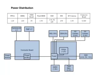
What needs to be powered? (1) All ASICs will be manufactured in an advanced CMOS (or BiCMOS) process, 130nm generation or below. Here we consider only CMOS ASICs. Detector module • Front-End readout ASIC • Idigital≥ Ianalog (for instance, current projection for ATLAS Short Strip readout is Ianalog~ 20mA, Idigital ~ 60-100mA) • 2 power domains: Van=1.2V, Vdig=0.9-0.8V (as low as possible) • Clock gating might be used => switching load Detector • Hybrid/Module controller • Ensures communication (data, timing, trigger, possibly DCS) • Digital functions only • It might require I/Os at 2.5V Read-out hybrid Rod/stave Other than the rod/stave controller, optoelectronics components will also have to be used, requiring an additional power domain (2.5-3V) F.Faccio, PH/ESE
What needs to be powered? (2) Large waste of power if Van=Vdig=1.2V Large current increase (Power on cables = RI2) • Summary • 3 Voltages to be provided to minimize power consumption: • 2.5V for optoelectronics and (maybe) control/communication ASICs • 1.2V for analog circuitry in FE ASICs • 0.8-0.9V for digital circuitry in FE ASICs. This domain uses most of the current! • Digital current might be switching in time (to really minimize the power) • Power and Current in LHC/SLHC • Projection based on current estimate for ATLAS upgrade • Only accounting barrel detector, power from Readout ASICs only • SCT is LHC ATLAS Silicon Tracker detector, to be replaced (grossly) by Short Strip layers in present upgrade layout (strawman design) F.Faccio, PH/ESE
Outline Power distribution in the trackers In LHC trackers Projection to SLHC – what needs to be powered? How to meet the new requirements HEP efforts to improve trackers Using DC-DC converters A proposed power distribution scheme Implementation of the scheme DC-DC converters basics (operation, losses) Comparison of different topologies Choice of topologies and estimated efficiency Challenges for successful development Radiation tolerance EMI (conducted and radiated noise) Conclusion F.Faccio, PH/ESE
I 10xI I 1xI 10xV, I V, 10xI DC-DC I 1xI 10xV Alternative distribution schemes • Different schemes are being investigated in HEP. They all decrease the current to be brought to the tracker. • Serial powering • Connecting modules with exactly the same current in series • Sizeable effort ongoing within ATLAS (strips and pixels) • Local voltage conversion • Using DC-DC conversion to provide correct voltage to the module/chip, while distributing higher voltage F.Faccio, PH/ESE
DC-DC conversion options • Switched devices • Cyclic transfer of energy from input to storing element, where it is used by the load • Different types: • Magnetic converters • Use of inductors to store energy • By far the most commonly used type of converter • Some work ongoing or planned in Yale & BNL (commercial components), • Switched capacitors converters • Use of capacitors to store energy • Mostly used to step-up the voltage (charge pumps), but step-down solutions are also found • Some work ongoing in LBNL (custom integrated component), PSI (on-chip converters) and INFN Florence (custom component with discrete devices) • Piezoelectric transformers • Use of ceramic materials to transfer energy from primary to secondary side, exploiting piezoelectric effect • No commercial step-down component available • Proposed by University of Tokyo within ATLAS in out F.Faccio, PH/ESE
HEP-specific requirements • Converters to be placed inside the tracker volume Magnetic field (up to 4T) Radiation field (>10Mrd) Environment sensitive to noise (EMI) • No commercial component exists, need for a custom development F.Faccio, PH/ESE
Magnetic field tolerance Max B CMS Minimum switching frequency Max B ATLAS Material We are forced to use coreless (air-core) inductors • This has a big impact on the available inductance magnitude, hence on the design of the converter F.Faccio, PH/ESE
Which inductor to use? • Air-core inductors can be manufactured in different configurations (planar, solenoidal, thoroidal, ….) and a choice should be made • Value: reasonably limited in range 100-700nH • Equivalent resistance (ESR) determines converter efficiency to sensible extent Planar (on PCB) Solenoidal Thoroidal ESR~100mW ESR~20-30mW ESR~20-30mW F.Faccio, PH/ESE
Proposed power distribution scheme “analog bus” 2.5V 10V “digital bus” 1.8V 2.5V (I/O) 0.9V (core) 1.25V (Vana) 1.25V (Vana) 0.9V (Vdig) 0.9V (Vdig) Controller ASIC Readout ASICs • Conversion stage 1 (ratio 4-5.5) • Vin=10V => high-V technology • Same ASIC development for analog and digital, only feedback resistive bridge is different • Conversion stage 2 (ratio 2) • Embedded in controller or readout ASIC • Closely same converter for analog and digital (different current, hence different size of switching transistors): macros (IP blocks) in same technology F.Faccio, PH/ESE
Implementation example 10V If Ihybrid<< Iout_converter If Ihybrid~ Iout_converter 2 Converter stage2 on-chip 2 Converter stage 2 on-chip 10V Detector Detector 2.5V 1.8V Detector 2.5V 1.8V Converter stage 1 2.5V Detector 1.8V 2.5V 1.8V 2.5V Optoelectronics 1.25V Stave controller Converter stage 1 on-hybrid 10V Converter stage 2 10V Converter stage 1 on-stave Rod/stave F.Faccio, PH/ESE
Summarizing proposed scheme • Components needed: • ASIC for conversion stage 1 (10V in, hence “high-V” technology) • ASIC macro (IP) for conversion stage 2 (in the FE ASIC technology) • Air-core inductor(s) • SMD Capacitances • Features • Conversion ratio close to 10 allows for considerably decreasing power loss on cables • Only 1 power line (10V) from off-detector, all other voltages generated locally • Capability to power both analog and digital domains with required voltage to minimize power – even in the event of switching loads • Only inefficiency due to conversion losses • High modularity • On-chip conversion stage allows in principle each ASIC to be turned on/off independently (power groups can also be envisaged): • Controller ASICs can be turned on first and alone – easy start-up condition • Depending on the modularity, defective FE ASICs (or groups) can be turned off to prevent the rest of the hybrid to be affected F.Faccio, PH/ESE
Outline Power distribution in the trackers In LHC trackers Projection to SLHC – what needs to be powered? How to meet the new requirements HEP efforts to improve trackers Using DC-DC converters A proposed power distribution scheme Implementation of the scheme DC-DC converters basics (operation, losses) Comparison of different topologies Choice of topologies and estimated efficiency Challenges for successful development Radiation tolerance EMI (conducted and radiated noise) Conclusion F.Faccio, PH/ESE
Vin-Vout Vout L L 2 1 L Vout Vin + - control Vout = Duty cycle load Vin Magnetic DC-DC converters basic • Schematic operation shown for the simplest topology: the buck converter IL t F.Faccio, PH/ESE
Ids with large Vds L Vout Vin Ron RL + - Ron control load 1/2fCV2 Losses in switching converters • Losses are responsible for inefficiency. They can be classified in: • Conductive losses • Switching losses • Driving losses • Losses in control circuit (generally negligible) gnd F.Faccio, PH/ESE
Different converter topologies (1/3) The following DC/DC step down converter topologies have been evaluated and compared in view of our specific application. • Single phase synchronous buck converter • Simple, small number of passive components • Larger output ripple for same Cout • Not suitable for high currents with available commercial inductors (limited in max RMS current) • 4 phase interleaved synchronous buck converter • Complete cancellation of output ripple for a conversion ratio of 4 (with small Cout) • Smaller current in each inductor (compatible with available commercial inductors) • Large number of passive components • More complex control circuitry L1 Vin Vout Q1 Rload Q2 Cout L1 Vin Vout Q1 Q2 L2 Rload Cout Q3 Q4 L3 Q5 Q6 L4 Q7 F.Faccio, PH/ESE Q8
i g Q 1 i C r 1 Q I L 2 o r V g + D v C 1 r + r v Load C o 2 D 2 Different converter topologies (2/3) • Two phase interleaved synchronous buck converter with integral voltage divider • Complete cancellation of output ripple for a conversion ration of 4 (with small Cout) • Simpler control and smaller number of passive components than 4 phase interleaved • Multi-resonant buck converter • Very small switching losses (zero voltage and zero current switching) • To achieve resonance: • Current waveforms have high RMS value => high conductive losses => lower efficiency • Voltage waveforms have high peaks, possibly stressing the technology beyond max Vdd • Different loads require complete re-tuning of converter parameters F.Faccio, PH/ESE
i g Q + 1 i C x 1 Q I 2 o + V v g x C Q x 3 + v Load C o 2 Q 4 Different converter topologies (3/3) • Switched capacitor voltage divider • rather simple , limited number of passive components • lack of inductor => good for radiated noise and for compact design • No regulation of the output voltage, only integer division of the input voltage • Efficiency decreases with conversion ratio (larger number of switches) • Good solution for ratio = 2, for which high efficiency can be achieved F.Faccio, PH/ESE
Conversion stage 1: topology Waveforms of the different topologies have been computed with Mathcad, and conversion losses have been estimated for each of them in the same conditions: Vin= 10V, Pout= 6W, Vout= 2.5V (step down ratio = 4), use of AMS 0.18um technology (vertical transistor) with approximate formula to account for switching losses The best compromise in terms of efficiency, number of components required, complexity and output ripple is the 2 phase interleaved buck with integrated voltage divider. F.Faccio, PH/ESE
Conversion stage 1: frequency For the chosen topology, more accurate calculations in different technologies (AMIS 0.35, AMS 0.18) have been carried out. This time switching losses have been estimated with dedicated simulation runs. Best results obtained with AMS 0.18 => all following calculations refer to this technology Quasi-Square-Wave (QSW) operation, where inductor current goes slightly negative at each cycle, turned out to be give higher efficiency in all cases (all switching but one are done in either zero-voltage or zero-current conditions) Note that Inductor value changes at each frequency and load condition to keep QSW operation. Inductor parameters taken from Coilcraft RF 132 Series For both “analog” (Vout= 2.5V) and “digital” (Vout= 1.8V) conversion stages, the highest efficiency is found for a working frequency of 1MHz. The curves below are for Pout= 6W. F.Faccio, PH/ESE
Implementation: conversion stage 1 • The final result of our study is that, for the development of a unique ASIC conversion stage 1 for both analog and digital power distribution, the best solution is: • 2-phase interleaved buck with integrated voltage divider • Switching frequency = 1 MHz • On-resistance of switching transistors = 30 mW • The inductor can be chosen for the specific output current wished in the application, achieving the efficiency estimated in the graphs below for the AMS 0.18 technology (Coilcraft RF 132 series inductors are used) DIGITAL, Vout=1.8V ANALOG, Vout=2.5V F.Faccio, PH/ESE
Implementation: conversion stage 2 Vin Q1 Q2 Vout=Vin/2 Q3 Q4 gnd • Two converters to be embedded on each chip • Output current rather modest (20-200 mA) • Inductor-based converters not envisageable: • With on-chip inductors (high ESR) the efficiency would be extremely low • The use of several discrete inductors per ASIC is not desirable – already only for system integration purposes • Switched capacitor converters more suitable • Acting as voltage divider (÷2) • They unfortunately do not provide regulation, which must be relied on from conversion stage 1 • Achievable efficiency has been estimated, then refined with a quick simulation in a 130nm technology (use of I/O transistors) • Efficiency (Vin=1.8V, Vout=0.9V, Iload=166mA, f=20MHz) = 93% • It should be pointed out that no study on the optimization of this converter has been made – one only topology, with one fixed frequency has been studied (efficiency can be improved further by decreasing the frequency, for instance). F.Faccio, PH/ESE
Efficiency of the two stages “analog bus” 2.5V, 4A 10V “digital bus” 1.8V,4A 2.5V (I/O) 0.9V (core) 1.25V (Vana) 1.25V (Vana) 0.9V (Vdig) 0.9V (Vdig) Controller ASIC Readout ASICs 90% 87% >93% >93% >93% >93% >93% Conversion stage 1 (ratio 4-5.5) Two phase buck interleaved with voltage divider Conversion stage 2 (ratio 2) switched capacitor voltage divider with ratio 2 • The efficiency of the two stages is equal to the multiplication of the efficiency of each stage: • Analog: 90%*93%=84% • Digital: 87%*93%=81% F.Faccio, PH/ESE
Projection for total power • Projection to SLHC ATLAS SS tracker • Comparison of SCT (present ATLAS strip tracker) and Short Strip strawman design for SLHC • Power loss in cables only for last Patch-Panel – at the edge of the tracker, in the hypothesis of 1W resistance on the return path per cable • For DC-DC conversion, we assume 10V input voltage to the stave/rod F.Faccio, PH/ESE
Outline Power distribution in the trackers In LHC trackers Projection to SLHC – what needs to be powered? How to meet the new requirements HEP efforts to improve trackers Using DC-DC converters A proposed power distribution scheme Implementation of the scheme DC-DC converters basics (operation, losses) Comparison of different topologies Choice of topologies and estimated efficiency Challenges for successful development Radiation field EMI (conducted and radiated noise) Conclusion F.Faccio, PH/ESE
Challenges: radiation field • The converter requires the use of a technology able to work up to at least 15-20V • Such technology is very different from the advanced low-voltage (1-2.5V) CMOS processes used for readout and control electronics, for which we know well the radiation performance and how to improve it • High-voltage technologies are typically tailored for automotive applications • Need to survey the market and develop radiation-tolerant design techniques enabling the converter to survive the SLHC radiation environment (> 10Mrd) • A 0.35mm technology has been extensively tested (see next slide) • In the near future, 3 other technologies will be tested in the 0.18-0.13mm nodes • Properties of high-voltage transistors largely determine converter’s performance • Need for small Ron, and small gate capacitance (especially Cgd) for given Ron! Prototypes in 0.35mm F.Faccio, PH/ESE
Irradiation results 0.35mm technology • Type of devices studied: • High-voltage transistors: • Vertical NMOS (rated 80V Vds, 3.3V Vgs), standard and ELT layout • Lateral NMOS (rated 14V Vds, 3.3V Vgs), standard and ELT layout • Lateral PMOS (rated 80V Vds, 3.3V Vgs) • Low-voltage (“logic”) transistors, standard and ELT layout for the NMOS • Irradiation with both X-rays (TID) and protons (TID and displacement damage) • Results: • Vertical NMOS: if ELT layout, TID is ok. BUT displacement damage dramatically increase Ron! • Lateral NMOS: if ELT layout, TID is ok. BUT this layout lead to failure to stand high voltage after proton irradiation. Different ELT layout needed, or rely on annealing… • Lateral PMOS: no leakage, BUT large increase of Vth with TID, and additional increase of Ron with displacement damage • Conclusion: • The use of lateral NMOS might possibly lead to a radiation tolerant converter, but the performance would not be very attractive (small efficiency) F.Faccio, PH/ESE
Outline Power distribution in the trackers In LHC trackers Projection to SLHC – what needs to be powered? How to meet the new requirements HEP efforts to improve trackers Using DC-DC converters A proposed power distribution scheme Implementation of the scheme DC-DC converters basics (operation, losses) Comparison of different topologies Choice of topologies and estimated efficiency Challenges for successful development Radiation field EMI (conducted and radiated noise) Conclusion F.Faccio, PH/ESE
EMC issues The switching converter can inject noise in the FE system it powers Conducted noise (via power cables) Radiated noise (EM field from inductor, loops, and switching nodes) The two are interlinked since any current in a loop radiates… EMI (dψ/dt) EMI (dV/dt) EMI (dI/dt) EMI (dI/dt) F.Faccio, PH/ESE
Conducted noise • Conducted EMI falls into two basic categories • Differential Mode, also called symmetric or normal mode • Common Mode, also called asymmetric or ground leakage mode Common Mode current in unshielded and badly grounded systems radiates > 3 orders or magnitude more than the same differential mode current. ICM IDM shield Power supply DC / DC Load ICM IDM Ground Plane F.Faccio, PH/ESE
Conducted noise measurement • Reference test bench developed within ESE • Well defined measurement methods for reproducible and comparable results. • Independence from the system and from the bulk power source. • Arrangement of cables, input and output filter (LISN) around the converter under test, all above a ground plane. F.Faccio, PH/ESE
Characterization of DC-DC prototypes • Several prototypes built and measured • Noise peaks at switching frequency (main) and harmonics • Similar result towards input and output Measurements with Vin=10V, Vout=2.5V, Iout=1A Output common mode current (dBmA) Frequency F.Faccio, PH/ESE
Characterization of DC-DC prototypes Prototype version 3 • Most recent prototype has much better noise performance • First integrated prototype (ASIC) also has good performance Measurements with Vin=10V, Vout=2.5V, Iout=1A Output common mode current (dBmA) Frequency F.Faccio, PH/ESE
Modeling common mode noise • A model for a prototype (version 3) has been developed and simulated with PSPICE • All stray capacitances due to the board layout have been extracted with Q3D • Switching transistors replaced by voltage source (from measured Vds) and equivalent passives (R,C) • All discrete passive components have been fully characterized (ESR, ESL) • Good agreement between model and experiment (up to 10MHz) • Large influence of input-output capacitors – value and ESR, ESL! Impact of ESR and ESL on input common mode noise current for Cin=40uF Output common mode current versus Cout value F.Faccio, PH/ESE
Radiated noise • Cyclic current variations in the inductor (dI/dt) generate a cyclic magnetic field (dB/dt) • Voltage (and current) develops on any loop crossed by dB/dt • For the FE readout circuits, the most sensitive loop is at the preamplifier input • Coupling mechanisms and curing strategies are under study • Measurements on TOTEM Si Strip modules using the VFAT readout chip • 3-D Simulation of magnetic field (Ansoft Maxwell) F.Faccio, PH/ESE
3-D simulation of magnetic field • Simulation of a Coilcraft 580nH inductor • DC current of 1A flowing in the inductor • Field intensity quickly drops with distance • At 1cm from the inductor, field is about 12mT F.Faccio, PH/ESE
Measurements on TOTEM modules • System: Totem Test Platform (TTP) with hybrid equipped with 4 VFAT and sensor (thanks to our TOTEM colleagues) • Disturbance generated by 538nH Coilcraft inductor with sinusoidal current of 1Apk at 1MHz • Inductor is moved in different positions F.Faccio, PH/ESE
Measurement on TOTEM modules • Work is on-going, no final result yet; only a few points worth summarizing: • No noise increase measured in hybrids without detector. As suspected, dominant coupling is at the input loop • Apparent noise when positioning the inductor on top of bonding and detector • Noise quickly decreases when distance is increased • Noise dramatically increase with frequency • Shielding with thin (>100mm) Al layer eliminates noise • Need to model the coupling mechanism: • How much is capacitive? • What is the loop and how we can minimize it? • How to shield efficiently and practically? F.Faccio, PH/ESE
Conclusion • Requirements of SLHC trackers call for new and more efficient power distribution system for better performance • The use of DC-DC converters on-stave/hybrid has the potential to meet the requirements • Converter topologies have been chosen for a proposed power distribution scheme with a total efficiency better than 80% • Special components needed: an ASIC in a high-voltage technology, an IP block, an air-core inductor • Prototype phase started (an ASIC buck converter exists and is being characterized) • Specific challenges in view of successful development: • Availability of radiation-tolerant high-voltage technology • Choice of appropriate inductor • EMI issues – mastering conducted and emitted noise • Scheduled end of the project: March 2011 F.Faccio, PH/ESE