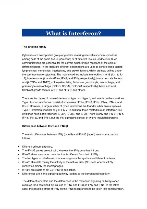
Plasmon Assisted Nanotrapping
280 likes | 600 Vues
Plasmon Assisted Nanotrapping. E. P. Furlani, A. Baev and P. N. Prasad The Institute for Lasers, Photonics and Biophotonics University at Buffalo, SUNY. Overview. Introduction Applications Experimental Results Modeling Nanotrapping Systems Summary. Optical Trapping – Laser Tweezers.

Plasmon Assisted Nanotrapping
E N D
Presentation Transcript
Plasmon Assisted Nanotrapping E. P. Furlani, A. Baev and P. N. Prasad The Institute for Lasers, Photonics and Biophotonics University at Buffalo, SUNY
Overview • Introduction • Applications • Experimental Results • Modeling Nanotrapping Systems • Summary
Optical Trapping – Laser Tweezers Powerful tool for remote manipulation of microscopic biomaterial. Strongly focused laser beam creates gradient optical force that traps particles. Not ideal for nanoscale trapping (diffraction limitation, heating). Not well suited for integration with Lab-on-Chip systems (opto- fluidics). D. G. Grier Nature 424 2003
+- +- +- +- Plasmonic-based Optical Nano-trapping Locally enhanced field near illuminated metallic nanostructures creates gradient optical force that traps nanoparticles. Einc(t) DielectricNanoparticle p Well suited for trapping sub-wavelength metallic or dielectric particles. Potential for integration with Lab-on-Chip systems (opto-fluidics). Gold Nanocones
E Strong Local Field d - - - - - - - - - + + + + + + m H . E(t) - - - + + + + + + - - - Surface Plasmon Resonance (SPR)and Localized SPR (LSPR) in Metallic Nanostructures Plasmon: Quantized charge density wave in free electron gas. SPR: Surface plasmons confined to metal/dielectric interface. Wave vectors LSPR: Resonant scattering modes in sub-wavelength metallic nanoparticles
Motivation for LSPR Nanotrapping • Higher Resolution: optical nano-manipulation of sub-wavelength particles (d << ) (overcome diffraction limit). • Reduced Power: optical intensity an order of magnitude lower then conventional optical tweezers • Multiplexed Nano-trapping: multiplexed parallel manipulation of particles using arrays of metallic nanopaticles • Microsystem Integration:integratedoptical particle manipulation/separation for BioMEMS, Lab-on-a-Chip systems.
- - - + + + + + + - - - Local Field Enhancement Metallic Nanoparticles E(t) d mp P(t) = E(t) Optical Absorption - Scattering Local Field Enhancement Absorption frequency/bandwidth depend on particle size, shape, composition and surrounding media etc.
Analytical Dielectric Function for Au Nanostructures +- +- +- +- Experimental and analytical dielectric values vs. Einc Analytical Dielectric Function for Au used in Analysis* *P. G. Etchegoin et al. J. Chem. Phys. 125, 164705 (2006)
Optical Trapping of Sub-Wavelength Neutral Particles Force on Dielectric Nanoparticle caused by Local Field Gradient produced by Illuminated Metallic Nanoparticles Dielectric Nanoparticle Metallic Nanostructures
Fabricated Metallic Nanostructures Nano-cone Array Nano-Ring Array Nano-Pillar Array T. Atay et al.,Nano Letters 4 2004 J. Aizpurua et al., PRL 90 2003
90 nm 120 nm Experimental Results Optical trapping of nanoparticles using taperedmetallic nanopillars 1 m Collaboration with A. N. Grigorenko et. al, Nanometric optical tweezers based on nanostructured substrates, U. Manchester UK
90 nm 120 nm Optical Trapping of Microbubbleson Nanostructured Substrate A.R. Sidorov et al.Optics Communications 278 (2007)
Moving Dielectric Sphere Trapped Dielectric Sphere Array of Au Nanostructures Enhanced Optical Trapping Au Nanoparticle Array X. Maio and L. Y. Lin, Opt. Letters. 32 2007,also unpublished work 2008
Array of Au Nanostructures Plasmonic Trapping of Cells Single Yeast Cell Trapped in Square (other cells moving at constant speed) Optical intensity required for stable trapping of single yeast cell is 78.8 W/m2 Moving Cells Trapped Cell X. Maio and L. Y. Lin, IEEE J. Sel. Topics Quant. Elec. 132007
Modeling Optical Nanotrapping • Dielectric Model for Metallic Nanoparticles. • Predict EM Field (Full-Wave Time-Harmonic Analysis) • Compute Time-averaged Optical Force Fopt on Dielectric Nanoparticles (Dipolar Force) • Identify Regions of Trapping • Use Fopt to Predict Particle Motion.
Optical Force on a Dielectric Nanoparticle Einc(t) p p +- +- +- +- d mp() mp() Time-averaged Optical Dipolar Force Fopt is a function of several variables: , p, mp(),d,and the geometry, composition and coupling of metallic nanostructures.
Trapping and Scattering Force Components Trapping Potential Vtrap:
Full-Wave Time-Harmonic Analysis(Array of Nanopillars: Glass Substrate covered with H2O) k y x p k z y x Computational Domain PML H2O PEC 3.4 m Glass 2 m PMC PML 2 m 2 m Symmetry Boundary Conditions: PEC, PMC
Computational Model y x p k z y x Surface current Jx BC chosen to produce plane wave: Ex = 2106 V/m. FEA Model: 43,904 cubic vector elements with 838,485 degrees of freedom. Computational Domain CPU Platform Dual Processor (3 GHz)Quad Core Windows XP 64 Bit32 GB Ram Time: 15 min per given Jx PML Incident Intensity5.3 mW/m2 H2O PEC 3.4 m Glass PMC PML 2 m 2 m Symmetry Boundary Conditions: PEC, PMC
Axial Optical Forcevs. Field Polarization Trap Einc TE TM k k TM polarization Trap k p Fz along this line H2O Glass
Rp = 50 nm = 1000 nm Einc TE Trap TM k p k Optical Force Analysis TE Analysis TM Analysis -<We>J/m3 -<We>J/m3 TE Analysis TrappingPotential Force Vectors in x-y Plane H2O H2O Glass Glass
Einc TE TM k d p k k Trapping Force Analysis TE Polarization = 635 nm Force vs. Cone Separation Force vs. Particle Size Rp = 50 nm No Trapping for Large ParticlesScattering Force Dominates
Axial Optical Forcevs. Field Polarization Trap Einc TE TM k k Fz along this line Trap H2O Glass k p
Induced Electromagnetic Modes = 635 nm -+ -+ Top View +- +- - - - - - - + + + + + + = 1000 nm Side View Top View – Induced Ez x Induced Ez E(t) -z
Rp = 100 nm Trap Einc TE Analysis k Glass/Air TE TM k Rp = 100 nm Trap TE Analysis Glass/H2O k p 2D Array of PillarsTE Trapping vs. Fz along this line H2O Glass
Rp = 100 nm Trap Einc Air Only TE TM k k k Rp = 100 nm Trap Glass/H2O p 2D Array of RingsTE Trapping vs. Fz along this line 300 nm H2O 200 nm 600 nm Glass
Summary and Conclusions • Optical trapping of neutral sub-wavelength particles can be achieved using local field enhancement near illuminated metallic nanostuctures. • Nano-trapping can be achieved with plane wave illumination. • Trapping force depends on particle size, , polarization and background permittivity. • Integration in Lab-on-Chip applications: Opto-fluidics