Download
1 / 7
80 likes | 240 Vues
This tutorial by Daryoush Shiri at the Institute for Quantum Computing (IQC) provides an in-depth look at the role of nanowires in quantum information processing. Covering essential topics such as electronic structure calculation, phonon spectrum, electron-phonon scattering, and spin-orbit interactions, the course highlights the advantages of using semiconducting nanowires as hosts for quantum dots. It discusses scalability, electrostatic control, and fabrication methods, making it a valuable resource for understanding the future of qubits and quantum computing technology.

E N D
QIC 890/891: A tutorial onNanowires in Quantum Information Processing DaryoushShiri, Institute for Quantum Computing (IQC) July 21, 23, 28 and 30, 2014
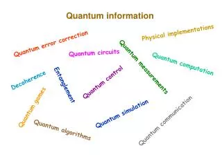
Agenda • Introduction • A crash course on • Electronic structure calculation • Phonon spectrum • Electron-phonon scattering • Spin-Orbit Interaction • Rashba term • Dresselhaus term • Exchange Interaction • Spin relaxation mechanisms • Dyakonov- Perel • Elliot - Yafet • Hyperfine interaction Daryoush Shiri, IQC
Introduction • Electron spin is a natural choice for a Qubit. • Spin of electrons in Quantum Dots (QD). • QDs are defined by potential landscaping on 2DEG. • 2DEG bandgap engineering in a superlattice. Spin to charge conversion ESR Electric Field (spin-orbit interaction) DaryoushShiri, IQC
Nanowires & QIP • Semiconducting nanowires • A Host for embedding interacting Quantum Dots • Topology-based Q-Computing: Hunt for Majorana Fermions • Emitters of single photon, entangled photons J. Baugh, IQC L. Kouwenhoven, Delft G. Weihs& H. Majedi, et al.
Superconducting nanowires • Detection of single photon (SNPD) NIST See courses offered by: Sir. Anthony Leggett and other faculty members at IQC and Physics on superconductivity
Why nanowires? • Compatibility with mainstream electronic chip industry • As opposed to 2DEG based Qdot systems: Scalability of Qubits • Embedding many Qdots (spin qubits) • Better electrostatic control (potential landscape) using many gates • Bandgap engineering Fabrication methods (1) Bottom-up methods e.g. VLS (2) Top-down methods • Group III-V (InP, InAs, InSb, GaAs, GaP, AlGaN,….) • Group V (Si/Ge) • Group II-VI (ZnSe/ZnTe) Review article by: J. Ramanujam, D. Shiri, and A. VermaMater. Express 1, 105-126 (2011).
Materials of Choice http://www.ioffe.rssi.ru/SVA/NSM/Semicond/ J. Baugh, IQC InAs InSb m*/m0 = 0.014 µe = 10,000 ~ 30,000 @ base temp (100mK) Lande’ g-factor = 50 m*/m0 = 0.023 µe = 10,000 ~ 30,000 cm2/V.s @ base temp (100mK) Lande’ g-factor = 10 λ MFP ~ 300nm Core-Shell InSb Tandem