Download
1 / 26
260 likes | 264 Vues
This article discusses the advancements in technology and the need for precise time measurements in electronics engineering. It explores different time measurement techniques and proposes using waveform digitization and constant fraction discrimination algorithms for high-performance time-to-digital converters. The article highlights the importance of signal-to-noise ratio and bandwidth in achieving precise time measurements.

E N D
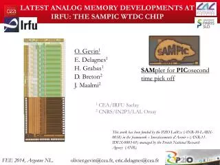
Designing fast analog memories for precise time measurementD.Breton (LAL Orsay)
Introduction The technologies have evolved at an amazing rate in the last decade, and during this period our electronics engineer everyday work has been transformed consequently Sometimes we have to build systems housing only few channels, but more often a lot, thus pushing us to look for the best solution to perform as precise as possible signal measurements at the lowest cost and power consumption, in order to be able to build large scale systems Our consecutive developments thus made us use high-end commercial ADCs and TDCs as well as developing high performance analog memories Now we deal with GS/s, which actually permits getting closer to ps => we can build high-end TDCs using waveform digitization …
About TDCs … Existing electronics for time measurement is mostly based on Time to Digital Converters (TDC). A TDC converts the arrival time of a binary signal into digital value. It is characterized by : Its time step and its main clock frequency Its effective resolution (which can be very different from time step) Its dead-time and its mean maximum hit rate Its number of channels Very few high-end products on the market, mostly dedicated to LHC HPTDC from CERN => 25ps & 40MHz TDC-GPX from ACAM => 8 channels, 80ps & 40MHz There is an important demand for time of flight measurement in the medical community, and now for ps precision in high energy physics
TDC with voltage ramp: => best solution for precision Time resolution: ~ 10 ps Usually used with a Wilkinson ADC for power and simplicity reasons => limited by dead time which can be a problem for high rate experiments TDC with digital counters and Delay Line Loops (DLL): => advantage: produces directly the encoded digital value but limited by delay line step - Time resolution of today’s most advanced ASICs: ~ 25 ps State of the art for TDCs BUT a TDC needs a binary input signal • analog input signal has to be translated to digital with a discriminator • overall timing resolution is given by the quadratic sum of the discrimator and TDC timing resolutions
New TDC developments There are very few new developments in the highprecision TDC area University of Alberta worked on using the HPTDC at 80MHz and achieved 15ps of resolutionusing custom CFDs CERN envisaged a new DLL-based TDC targetting 15 ps of resolution Anyhow, the standard DLL-based option islimited by the time propagation step in the DLL and the factthat one cannotinterpolatethis information Usual trick for improving the precision: interleavingDLLsfedwith phase shiftedsignals Onlyway to furtherincrease the precisionis to run for smaller technologies But single delaystepwillhardly go below a few 10 ps And if one wants to keepreasonableclockfrequencies in the chips (used for rough time counters), DLLswillremain long => bad for precision
ADC and TDC The best way to precisely measure the arrival time of a signal is to digitize it with a very fast and precise ADC. Indeed, once data is digitized, one can perform a digital treatment of data to precisely extract time information Waveform contains all information (if properly digitized) Depending on the information requested (amplitude, charge, time, FFT, …), different types of algorithms can be used Goal is to find the both simplest and most effective algorithms which can be integrated within companion FPGAs Waveform sampling can be used for designing high performance TDCs It was shown that 5-10GS/s sampling rate together with a good SNR (>10bits) was leading way to the ps level Signal to noise ratio is always an issue, even for a TDC
The easiest way to extract the time information from a digitized signal is to perform a digital Constant Fraction Discrimination (CFD) Indeed, a simple threshold method introduces Time Walk which depends on the signal amplitude in order to remove the time walk, threshold has to be set as a constant fraction of the signal amplitude Algorithm can be as simple as looking for the closest sample to the peak and performing a linear interpolation between samples around the threshold => easy to implement within a FPGA. More complex algorithms based on multi-sample digital filtering may improve the resolution Extracting the time from the signal: CFD A1 V V relative threshold : constant fraction of the peak! A2 A3 k x A1 Fixed threshold k x A2 k x A3 t t Δt : time walk Δt ~ 0
Noise Time Time Jitter Jitterinduced by electronics noise Simplified approach slope = 2ЛAf3db tr ~ 1/(3 f3db) Zoom Jitter [ps]~Noise[mV] / Signal Slope [mV/ps] ~tr / SNR Ex: the slope of a 100mV - 500MHz sinewave gets a jitter of ~2ps rms from a noise of 0.6mV rms • Conclusions: • The higher the SNR, the better for the measurement • A higher bandwidth favours a higher precision (goes with its square root). • But: for a given signal, it is necessary to adapt the bandwidth of the measurement system to that of the signal in order to keep the noise-correlated jitter as low as possible • Designs become tricky for ultra fast signals with a bandwidth > 1GHz …
ADC-based TDC The best digitizer would be a low-power flash ADC running at a rate >> GS/s over a lot of bits (12) Because every single sample would have followed the same path: Sampled by the physical same clock (thus with an excellent jitter performance) Digitized by the same elements => thus avoiding any dispersion due to layout non-uniformities This doesn’t exist => very fast ADCs are based on a bank of parallel ADCs => they require an internal complex calibration => they consume quite a lot of power The output dataflow of these circuits makes them very difficult to use The most powerful products on the market: 8bits => 3GS/s, 1,9 W => 24Gbits/s, 10 bits => 3GS/s, 3,6 W => 30Gbits/s 12 bits => 3,6GS/s, 4,1 W => 43,2Gbits/s 14 bits => 400MS/s, 2,5 W => 5,6Gbits/s
An actual 12 bits and 3.6GS/s … BGA 292 pins Output links: 24 x1,8Gbits/s 1.8 GHz ! • Need of a VERY high-end FPGA • power, cost, board design complexity, … • and what about radiation if any ?
Why Analog Memories ? Analog memories actually look like perfect candidates for high precision time measurements at high scale: Like ADCs they catch the signal waveform (this can also be very useful for debug) There is no need for precise discriminators TDC is built-in (position in the memory gives the time) Only the useful information is digitized (vs ADCs) => low power Any type of digital processing can be used Only a few samples/hit can be read => this may limit the dead time Simultaneous write/read operation is feasible, which may further reduces the dead time if necessary Main difficulty is less sampling frequency than signal bandwidth But their design is tricky if one wants to reach the necessary level of performance.
Basic principles of circular analog memory • A write pulse is running along a folded delay line. • Sampling stops upon trigger. • Readout can target an area of interest: • Starting from Trigger cell (marked during signal • recording) - programmable offset (linked to latency). • Total readout can however be necessary. • Read Cell index necessary. • Dead time due to readout has to remain as small as • possible (<100ns / sample).
Main design options The choices of architectures are different depending on the recording options. Main options: Pure waveform recording (can cover a long time period) => can be used for rough time measurement. Precise time measurements. It looks like both are not achievable with the same designs The ps level relies on the quality of the sampling then in the capacity to easily correct the remaining fixed sampling errors Of course the better original sampling, the easier The calibration has to remain reasonable, as well as necessary correction of data
Targetting the ps … • As said before, a perfect digitizer would be for instance a 10GS/s 12-bit flash ADC. • But 10GS/s sampling doesn’t give enough time to work on the sampled signal (100ps for sampling + transfer ) • Moreover, the 120Gbits/s output data rate could make anybody nauseous … • the idea is to keep the high sampling rate and to increase the time for processing the samples by parallelizing the operation via the Sampling Delay Line • There will be as many sample and hold cells as delays in the line • This increases the time allowed for sampling the signal (write pulse can cover many consecutive delay cells)
Basic scheme Pros: very simple and easy to implementscheme Cons: time propagation is not servocontrolled => individualdelays have to becalibrated and mayvarywith time and temperature
Fake signal Δt[cell] Real signal After interpolation Time Non_Linearities • Dispersion of single delays => time DNL • Cumulative effect => time INL. Gets worse with delay line length. • Systematic & fixed effect => non equidistant samples => Time Base Distortion • If we can measure it => we can correct it ! • But calibration and even more correction have to remain “reasonable”. In a Matrix system, DNL is mainly due to signal splitting into lines => modulo 16 pattern if 16 lines Remark: same type of problem occurs with interleaved ADCs
Improved scheme Here, time propagation isservocontrolled => individualdelays are much more precise and should not varywith time. However, if the Delay Line istoo long, integral non linearitymaybe important
How to use it ? Here, output rate = input rate => thisactuallyis an ADC ! Actually, mostADCsintegrated in high-end oscilloscopes’ front-end workthatway ! Fclock/Nb of delays
Dual-stage analog memory Here, output rate = input rate only for the first stage Difficultyis to copy the sampled signal veryproperlybetween the two stages Short first stage is fixing the time precision performance but transfermay damage the information
Towards a ps TDC … In order to build a real TDC targetting the ps level, adding an analog memory to a usual DLL TDC permits relieving the walk constraint on the discriminator and improving the time precision by an order of magnitude Here the Delay Line is servo-controlled and can be as short as the signal to measure => very good time resolution can be envisaged Critical path for time measurement
Remarks The technology choice depends on the design. It might be good not to chose too complex or expensive technology if this is not necessary Following the trends might be risky There are many cheap and good “old” technologies An important element is the channel occupancy The architecture has to be adapted to the required channel hit rate Waveform sampling means that a certain amount of cells has to be readout for each hit reconstruction => Intrinsic deadtime If the readout scheme becomes too difficult to implement, reducing the pixel size and increasing the number of channels might be a solution But then the overall number of channels will follow => try to increase the number of channels within one chip
Remarks (2) The analog memory could also be used as a first level derandomizer Either individual cells or banks of cells could be frozen waiting for readout while sampling goes on This implies a simultaneous write/read operation in the memory potential source of crosstalk, noise, distorsion … critical design but if the derandomizer depth is sufficient, the memory could get close to zero deadtime When the ps is the goal, the clock distribution becomes a problem by itself, especially for high scale systems The board design also becomes really difficult, mixing high bandwidth analog front-end and fast digital logics
Memory-associated ADC Sampled analog waveform has to be digitized ADC can be internal to the chip, or external External: The simplest solution: multiplexing all the samples towards a single ADC Cheap but induces a relatively high dead-time The most effective in terms of dead-time: driving many ADCs in parallel (can be multi-channel ADCs) Internal: The simplest solution: the Wilkinson ADC Can be parrallelized (ramp and counter can be shared) Can be partly inside (ramp and comparator) and outside the chip (counter located in the companion FPGA) Counter can be embedded in each cell Smart implementations highly increasing the speed can be used (WILKY) The main problem with internal ADC: extracting rapidly the digital data => this could really become problematic for dense circuits
Advanced integrated ADC design: WILKY • New ADC development based on boosted Wilkinson architecture. • Use of DLL-based digital TDC techniques to measure the time in a ramp ADC (patented in 2005) • Equivalent to a Wilkinson ADC with a 3.2 GHz clock. • 4-channel prototype validated in 2006 in CMOS 0.35µm technology • Easily expendable to 64 channels or more Raw Time: counter Fine Time: DLL
Summary Waveform sampling can be used for designing high performance TDCs ADCs would do the job nicely but at least 99% of data would go to the bin at owner’s expense! (power, FPGA, …) Analog memories actually look like perfect candidates for high precision time measurement at high scale and reasonable trigger rates: Design has to be adapted for such a requirement (short servo-controlled sampling delay lines) Not only high sampling precision but high SNR is mandatory 1GHz of bandwidth currently looks like a technical boundary if one wants to keep a low signal distorsion But this should already permit reaching the ps level