Physics of Semiconductor Nanostructures
690 likes | 1.55k Vues
Physics of Semiconductor Nanostructures. 鄭舜仁 ( http://www.cc.nctu.edu.tw/~sjcheng/Frameset05.htm ) Department of Electrophysics, National Chiao Tung University. 2006 Spring Semester. Reference Books & Articles:

Physics of Semiconductor Nanostructures
E N D
Presentation Transcript
Physics of Semiconductor Nanostructures 鄭舜仁 (http://www.cc.nctu.edu.tw/~sjcheng/Frameset05.htm) Department of Electrophysics, National Chiao Tung University 2006 Spring Semester Reference Books & Articles: [1] "The physics of low-dimensional semiconductors: an introduction", by John H. Davies, Cambridge university press (1998). URL: http://userweb.elec.gla.ac.uk/j/jdavies/ldsbook (Chapter 1,3,4,6,9,10) [2] Thesis “Correlations in semiconductor quantum dots” , Marek Korkusinski, June 2004, University of Ottawa (Chapter1,2,3 ) [3] Thesis “Collective Excitations and Coulomb Drag in Two-Dimensional Semiconductor Systems” , Shun-Jen Cheng,September 2001, Universität Würzburg (Chapter2 ) [4]“ A Guide to Feyman Diagrams in the Many-Body Problem, R.F. Mattuck (Dover Books) (1992) [5] “Electronic structure of quantum dots”, S. M. Reimann and M. Manninen, Reviews of Modern Physics, 74, 1283 (2002) [6] “Magnetism in condensed matter”, Stephen Blundell, Oxford University Press (2001) (Chapter 1 &2) [7] “Quantum theory of the optical and electronic properties of semiconductors”, H. Haug and S. W. Koch, World Scientific (Chapter 1) [8] “Excitonic artificial atoms: engineering optical properties of quantum dots”, Pawel Hawrylak, Phys. Rev. B 60, 5597 (1999). Evaluation:1. Exercises: 50% 2. Oral presentation: 50%
Gate-defined dot Mesa-etched dot 1m~100nm Self-Assembled Quantum Dots - + Three-dimensional STM image of an uncovered InAs quantum dot grown on GaAs(001). J. Marquez, et al, Appl. Phys. Lett. 78 (2001) 2309. - - - - - - - - - - Semiconductor nanostructures 1µm~100nm ~20nm ~20nm Quantum ring
Semiconductor nanostructures Colloidal nanocrystals ~few nm
Carbon nanotubes: One dimensional system Here are some real-world nanotube materials, produced by laser ablation of a graphite target containing metal catalyst additives. On top is an atomic force microscopy image of a chiral tube with a diameter of 1.3 nanometers (Technical University, Delft: www.pa.msu.edu/cmp/csc/nanotube.html). (Courtesy Cees Dekker, Delft Institute of Technology, the Netherlands.) This research was reported in the 7 May 1998 issue of Nature.
Outline Outline:1. Introduction to semiconductor nanostructures [1,2](1w) 2. Formation of semiconductor nanostructures [1,2](0.5w) gate-defined quantum dots (QDs) self-assembled QDs synthesized nanocrystals (NCs) quantum wires, quantum rings… 3. Single-particle properties [1,2,3](2w) band theory in solids k.p theory envelope function approximation quantum disk parabolic model spherical quantum dots (QDs) quantum rings* strain effects * asymmetric nanostructures 4. Electric and magnetic fields [1] (1w) nanostructures in magnetic fields nanostructures in magnetic fields :Stark effects Fermi’s golden rule The Aharonov-Bohm effect* Quantum Hall effects in 2D and 0D systems* 5. Many-particle problems [1,4] (3w) Hartree & Hartree-Fock approximation(0.5w) Second quantization(2.5w) Configuration interaction method Technique of exact diagonalization* Many electrons in QDs 6. Transport properties[5,6] (2w) Coulomb Blockade spectroscopy(1w) Hund’s rule(1w) Quantum Hall droplets in QDs* 7. Optical properties[1,7,8](2w) Dipole approximation & Fermi’s golden rules emission and absorption spectrum Fine structure of the optical spectrum of QDs 8. Magnetic properties[6](2w) Magnetism of QDs Semi-magnetic QDs Spintronics 總授課時間約14週 Oral presentation: 2週 Home work: 4~6次 [#]: reference#; *: optional; (nw): n weeks
Outline Outline:1. Introduction to semiconductor nanostructures [1,2](1w) 2. Formation of semiconductor nanostructures [1,2](0.5w) gate-defined quantum dots (QDs) self-assembled QDs synthesized nanocrystals (NCs) quantum wires, quantum rings… 3. Single-particle properties [1,2,3](2w) band theory in solids k.p theory envelope function approximation quantum disk parabolic model spherical quantum dots (QDs) quantum rings* strain effects * asymmetric nanostructures 4. Electric and magnetic fields [1] (1w) Electrostatic potential Stark effects Fermi’s golden rule The Aharonov-Bohm effect* Quantum Hall effects in 2D and 0D systems* 5. Many-particle problems [1,4] (3w) Hartree & Hartree-Fock approximation(0.5w) Second quantization(2.5w) Configuration interaction method Technique of exact diagonalization* Many electrons in QDs 6. Transport properties[5,6] (2w) Coulomb Blockade spectroscopy(1w) Hund’s rule(1w) Quantum Hall droplets in QDs* 7. Optical properties[1,7,8](2w) Dipole approximation & Fermi’s golden rules emission and absorption spectrum Fine structure of the optical spectrum of QDs 8. Magnetic properties[6](2w) Magnetism of QDs Semi-magnetic QDs Spintronics 總授課時間約14週 Oral presentation: 2週 Home work: 4~6次 [#]: reference#; *: optional; (nw): n weeks
Introduction to semiconductor nanostructures • Semiconductor (SC). • Fabrication • Scale of nanometer. • Interesting Physics in SC nanostructures: - transport measurement - optical spectroscopy - magnetic (& spin) properties • Observations & Measurements • Possible Applications
What’s “structure”? What’s “nano-scale”? Why nanostructures? Why study the physics? What’s interesting physics? How to study the physics? Understand better the physics, then… What’s SC? Why SC? Physics of Semiconductor Nanostructures
Band Diagram of Solids Single atom Solid 3s N conduction band 2p 6N Valence band Energy 2s 2N 2N 1s position
T>0 doping + + + + + + Metal, Insulator, and Semiconductor metal insulator semiconductor Conduction Band (CB) Energy gap (Eg) Valence Band (VB)
Semiconductor Heterostructures* * 2000 Nobel prize in physics Confinement potential
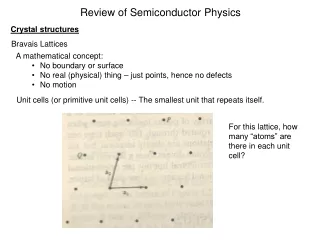
Length scales in semiconductors (SC’s) Lattice constant: (see “Electronic transport in mesoscopic systems”, S. Datta, Cambridge Univ. Press) 100m lF of bulk: Mean free path: 10m Effective Bohr Radius: Coherent length: E 1m 100nm mesoscopic 10nm a 1nm 0.1nm Is Nanometer small or large?
Low-Dimensional Systems <<100nm, in usual. Quantum Well (quasi-2D) Quantum Wire (quasi-1D) Quantum Dot (quasi-0D)
Formation of Quantum Dots Gate-defined dot Pillar dot 1m~100nm etching 1m~100nm - + - - - - - - - - - - Self-assembled dots ~10nm
Aspects of Nanostructures bulk Room temp. kT~25meV Nano-Technology dN/dE (density of states) ~100meV (for GaAs) 10nm Nano-scale Semiconductor nano-technology, Material engineering, etc… E Advanced Applications Fundamental Interest Quantum-dot lasers, Photodetectors, Single electron devices, Single photon devices, Quantum computing, etc…. Atom physics, Many-body physics, Quantum optics etc…..
Current transport through a classical resistance I I w V _ + V Conductance (G) W
Quantum Point Contact B.J. van Wees, PRL 60, 848(1988). (see also J.H. Davies Fig.5.22/p186)
Quantum Point Contact _ 5 ~250nm 4 Vg Vg 3 I h: Planck’s constant V 2 + 1 : metal (gate) Vg : two-dimensional electron gas W *see also quantum Hall effect (Nobel prizes in ’85,’98) p228 in textbook.
Quantum Point Contact (metal) Quantized conductance through individual rows of suspended gold atoms H. OHNISHI, et al., Nature 395, p780 (‘98) lF of metal: ~0.9nm
Coulomb Blockade in Quantum Dot (Q.D.) Quantum dot J. Weis, et al. Phys. Rev. Lett. 71, 4019-4022 (1993) Vg Vg G I “single” electron transister (SET) S D Vg S G D G (a review article about Q.D.: S.M. Reimann and M. Manninen, Review of Modern Physics, 74,1283 (2000))
dot Source Drain Vg Spin polarization Quantum Hall Droplet E B B T.H.Oosterkamp, PRL, 82, 2931 (1999) N-1 B
Photoluminescence (PL) from (parabolic) Quantum Well R.C. Miller, et al. Phys. Rev. B 29, 3740 (’84) Also see sec. 4.3 in textbook 40meV
PL from Ensemble of Quantum Dots Artificial atoms!!! ~20nm Sylvain Raymond and cowokers, NRC, Canada
Magneto-PL from Ensemble of Quantum Dots d+ B d d- p+ p- s Sylvain Raymond et al. PRL(2004)
Single-Dot PL Spectrum • Fermi’s golden rule • intitial state: ground state. • final state: GS & “all” excited states The interband polarization operator B=0 experiment theory X6 Gs-to-GS Hawrylak, Cheng M.Bayer et al, Nature405, 923 (2000)
PL from Single Quantum Dot 20meV ~20nm Robin Williams and cowokers, at NRC, Canada
Coulomb Blockade spectrum of a Single Nanocrystal U. Banin, Y. Cao,D. Katz, and O. Millo, Nature vol.400, 542 (1999) InAs NC
Calculation Experiment N=1 2 3 4 5 6 7 8 µ4
B M SQUID B B
B M SQUID Paramagnetism of QDs: experimental results CdMnSe QD Cd0.996Mn0.004Se PbSe QD B Low-field paramagnetism T Wen-Bing Jian et al, to be published Wen-Bing Jian et al
Observation of Nanostructures • Scanning Electron Microscope (SEM) Resolution>10nm * 10-40kV Electron beam * See, for instance, “University Physics”, by Harrison Benson, John Wiley & Sons, Inc.
Observation of Nanostructures Observation of Nanostructures • Transmission Electron Microscope (TEM) Electron beam 50-100kV diffraction Resolution>0.5nm
Observation of Nanostructures Three-dimensional STM image of an uncovered InAs quantum dot grown on GaAs (001). J. Marquez, et al, Appl. Phys. Lett. 78 (2001) 2309. Scannning Tunneling Microscope (STM)* * Nobel prize in 1986 I=const Resolution: 0.001nm (vertical) 0.1nm (horizontal)
Possible Applications 。Quantum dot infrared photodetectors, QDIPs -- Aslan, B.,Liu, H.C., Korkusinski, M., Cheng, S.-J., and Hawrylak, P., Appl. Phys. Lett. 82, 630 (2003) 。Optical memories --Petroff, P.M., in:Single Quantum Dots: Fundamentals, Application, and New Concepts, Peter Michler (Ed.) (Spring,Berlin,2003); -- Lundstrom, T., Schoenfeld, W. Lee, H., and Petroff, P.M., Science 286,2312(1999) 。Single-Photon sources --Michler, P., Kiraz, A., Becher, C., Schoenfeld, W.V., Petroff, P.M., Zhang, L., Hu, E, and Imamoglu, A., Science 290, 2282 (2000) --Moreau, E., Robert, I., Manin, L., Thierry-Mieg, V., Gerard, J.M., and Abram, I., Phys. Rev Lett. 87,183601 (2001) --Santori, C., Pelton, M., Solomon, G., Dale, Y., and Yamamoto, Y., Phys. Rev. Lett. 86, 1502 (2001) --M.Pelton et al, Phys. Rev. Lett.89, 233602 (2002)
Possible Applications 。QD lasers --Arakawa, Y., and Sasaki, H., Apl. Phys. Lett. 40, 939 (1982); Fafard, S., Hinzer, K., Raymond, S., Dion, M.,McCAffrey, J., Feng, Y., and Vharbonneau, S., Science 22, 1350 (1996); Maximov, M.V., Shernyakov, Yu.M., Tsatsul'nikov, A.F., Lunev, A.V., Sakharov, A.V., Ustinov, V.M., Egorov, A.Yu., Zhukov, A.E., Kovsh, A.R., Kop'ev, P.S.,Asryan, L.V., Alferov, Zh.I., Ledentsov, N.N., Bimberg, D., Kosogov, A.O., and Werner, P., J. Appl. Phys. 83, 5561 (1998); Ledentsov, N.N., Ustinov, V.M., Shchukin, V.A., Kop'ev, P.S., Alferov, ZH.I., and Bimberg, D., Semiconductors 32, 343 (1998); Fafard, S., Wasilewski, Z.R., Allen, C. Ni., Hinzer, K., McCaffrey, J.P., and Feng, Y., Appl. Phys. Lett.75, 986 (1999) 。Terahertz radiation --Anders, S., Rebohle, L., Schrey, F.F., Schrenk, W., Unterrainer, K., and Strasser, G., Appl. Phys. Lett. 82, 3862 (2003) --Apalkov, V.M. and Chakraborty, T., Appl. Phys. Lett. 78, 1820 (2001) --Wingreen, N.S. and Stafford C.A., IEEE J. Quant. Electron. 33, 1170 (1997) 。Single electron transistor, quantum computation,…