Download

1 / 24
290 likes | 499 Vues
Explore electron states in nanostructures, conductance concepts, and quantum transport phenomena. Dive into 2D, 1D, and 0D structures like graphene, carbon nanotubes, and more. Learn about electron effective mass, Schrödinger equation, and density of states in different dimensions.

E N D
Katherine Luna, Inspiration [online image] 23 Feb 2011, http://www.lorentz.leidenuniv.nl/inspiration/
Quantum transport in semiconductor nanostructures Thomas Ihn ETH Zürich FS 2017
Organisation Exercise classes: Hiske Overweg, overwegh@phys.ethz.ch Riccardo Pisoni, pisonir@phys.ethz.ch What you are supposed to do: • 1 oral presentation (10 min) in the exercise class • solve the problem sheets • active participation in lecture and exercise class (!) Website: http://www.nanophys.ethz.ch
Feedback... please feed back!
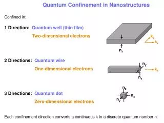
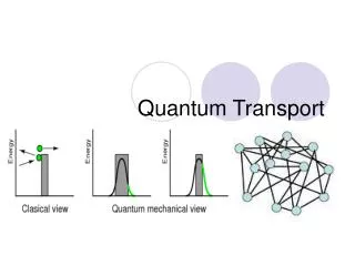
Today's lecture • Nanostructures in 2D – 1D – 0D • How we describe electron states • What is conductance really?
Nanostructures in 2D - 1D - 0D A.H. Castro Neto et al, Drawig conclusions from Graphene, Physics World (Nov 2006) [online], 22 Feb 2012, http://physics.bu.edu/~neto/Topic0.htm
Electrons in two dimensions 2004: • 90 nm technology • smallest gate length 50 nm • 5x10⁶ transistors/chip Si wafer IBM Switching speed: • channel length • drift velocity Pentium IV: • 42’000’000 transistors • 2 GHz strained-silicon transistor (IBM)
Electrons in one dimension Carbon nanotubes
Electrons in one dimension InAs nanowires Bi2Se3 nanoribbons: topological insulators
Electrons in one dimension Graphene nanoribbons
Electrons in one dimension GaAs quantum point contacts GaAs quantum wires by cleaved edge overgrowth
Electrons in zero dimensions AFM- lithography electron beam lithography growth on prepatterned substrates+self-assembly self-assembling growth
Band structure of GaAs and Si GaAs Si
Effective mass approximation (parabolic band) Quantum description: Schrödinger • Effective mass • Envelope functions Corresponding classical description: Newton
Our simplified quantum view on electrons effective mass Schrödinger equation
Quantum transport phenomena 1987 1980 1989 1980
Read until next week Chapters VI. Fabrication of nanostructures X.1-3 Drude model