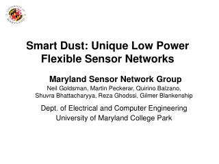
Smart Dust: Unique Low Power Flexible Sensor Networks
460 likes | 627 Vues
Smart Dust: Unique Low Power Flexible Sensor Networks. Maryland Sensor Network Group Neil Goldsman, Martin Peckerar, Quirino Balzano, Shuvra Bhattacharyya, Reza Ghodssi, Gilmer Blankenship Dept. of Electrical and Computer Engineering University of Maryland College Park.

Smart Dust: Unique Low Power Flexible Sensor Networks
E N D
Presentation Transcript
Smart Dust: Unique Low Power Flexible Sensor Networks Maryland Sensor Network Group Neil Goldsman, Martin Peckerar, Quirino Balzano, Shuvra Bhattacharyya, Reza Ghodssi, Gilmer Blankenship Dept. of Electrical and Computer Engineering University of Maryland College Park
Outline: Focus on Hardware for Achieving Smart Dust Motes and Working Network • Overview • Power Efficient Micro RF Circuits • Digital Low Power Circuits and Networking • Ultra Small Antennas • Energy: Micro Super Capacitor-Battery • Energy Harvesting: RF & RF
/power Overview: Smart Dust Hardware Smart Dust Node • Analog Transceiver • Microprocessor • Communication and Sensor Control • Decision making • Micro-Battery • Energy Harvesting • Micro-Antenna ~1mm Smart Dust Particle
Power Efficient Micro RF Circuits: Smart Dust RF Receiver and Transmitter Bo Yang, Thomas Salter Yiming Zhai and Neil Goldsman
Receiver Summary • Previous Review Results: • Tested initial OOK (On-off Keying) receiver without comparator. The output of receiver is not quite a digital signal. • Tested Low Noise Amplifier (LNA), performance is poor due to poor layout considerations. • Current Review Results: • Tested full OOK receiver. It can demodulate a modulated signal, and provide a ready to use rail-to-rail amplitude. • Tested the performance of LNA for its Gain (S21), Matching (S11 , S22) and linearity (IIP3, P-1dB). • Tested performance of on-chip comparator. • Measured our chip receiving and demodulation performance using our antenna (FICA). (See video file).
Receive Architecture:On-Off Keying Micrograph of actual chip
Minimum Detectable Signal Summary of Receiver Performance Operational with custom ultra-small FICA antenna
Micrograph and Performance of full OOK Receiver Measured gain and return losses of the LNA. Gain: S21 = 11.3 dB, Return Loss: S11 = -11.8 dB, S22 = -8 dB • Receiver operation verified • Signal extracted from noise • Modulated Input: green • Demodulated output: yellow
Power Amplifier Oscillator Buffer Transmitter
Transmitter Overview • Design a new CMOS ring oscillator and an LC oscillator • The new CMOS ring oscillator has wider frequency tunable range than the first version design • The new CMOS ring oscillator consumes much less power than the LC oscillator and has wider frequency tunable range • Improved gain of Power Amplifier with new layout
Voltage Controlled Oscillator Results CMOS Ring Oscillator VCO • Tuning range: 424MHz ~ 2.235GHz • Power consumption: 2.63mW @ 2.2GHz • About 80% of the power is consumed by the output buffer. Ring Oscillator Output CMOS LC VCO • Tuning range: 2.093GHz ~ 2.893GHz • Power consumption: 7.7mW @ 2.2GHz • About 27% of the power is consumed by the output buffer. LC Oscillator Output
New Power Amp Reduces Parasitic Losses & Increases Gain Resistive losses in initial Design Some Power Loss here (1.2 dB) Most of Power Loss Here (3.8 dB) PA was redesigned and taped out to reduce parasitics. Gain improved by 4 dB to a total gain of 17 dB, efficiency between 35 & 50%, depending on the inductors available in the process.
Digital/Low Power Design and Optimization of Smart Dust Sensor Nodes and Networks Chung-Ching Shen, Roni Kupershtok, Shuvra Bhattacharyya and Neil Goldsman
Digital Design Overview • Goal is to design and fabricate the digital component of the smart dust nodes. • Develop extremely low power ASIC (microwatts) • Develop small footprint (millimeter) • Integrate with analog sensor and transceiver • Develop and implement communication algorithms and sensing • Developing low power asynchronous design methods to eliminate clock trees
Digital Design: New Results Summary • Digital ASIC Design of the Smart Dust System • Designed a digital ASIC chip that performs protocol sensor control and inter-node communication for Smart Dust • This chip was designed for integrating On-Off Keying (OOK)-based analog transceiver modules. • Has less I/O interfaces resulting in smaller chip size • This design has been demonstrated in an FPGA, and also submitted to IBM 0.13µm fabrication. Overall project flow Software complete Partially complete FPGA Analog Digital ASIC mixed-signal ASIC design 16
Receive Packet Smart Dust ASIC Design • Schematic design of the ASIC • 8 major modules • 12 sub modules • All the modules have been implemented with Verilog. • All the modules have been tested and verified with an FPGA development platform. • Only one wire is needed to receive input bits from a wireless receiver. • Only one wire is needed to transmit output bits to a wireless transmitter. Packet Filter Clock Counter Control Unit Pre Sync Control S e n s e Core Transmit Packet 17
Process: IBM 0.13 µm Voltage: 1.32 V Target Freq: 20MHz Core : Dynamic Power: 10.7 µW Leakage Power: 554 nW Core Size: 2.8e+5 µm2 # of Gates: 6843 Chip Size: 10.5e+5 µm2 Pads: 20 (includes test pins) The Layout Snapshot and Design of the Smart Dust Digital ASIC 18
Experimental Platforms and Results • FPGA-based system prototype • FPGA (for demonstrating Smart Dust ASIC Design), LINX OOK-based transmitter/receiver, line crossing 19
Experimental Platforms and Results 2cm Previousprototype PCB: 2cm X 3cm 3cm 15mm 15mm The latestprototype PCB: 1.3cm X 1.3cm (only lower left corner used) 1.5x1.5x1.5cm3 Smart Dust Mote 1.3cm World’s Smallest 2.4GHz mote, to our knowledge 1.3cm Compact size smart dust system design 20
FICA: F-Inverted Compact Antenna Ultra Small Antenna (<< l/4) Bo Yang, Xi Shao, Quirino Balzano, Neil Goldsman January, 2008
Review Summary • Last Review: • Improved design of FICA • Measured Gain performance of 916 MHz FICA • This Review • Fabricated FICA for 2.2 GHz with 1.1 cm x 1.1 cm ground plane. • Fabricated FICA for 2.4 GHz with 1.1 cm x 1.1 cm ground plane. • Tested 2.2 GHz FICA outdoor. • Measured FICA performance with in-house designed On-Off Keying (OOK) receiver • Developed circuit model of FICA • Expected 3D integration of transceiver, with lowest form factor in the world • Investigation of ground plane size effect under way
2.2 GHz FICA Gain Test (I) • Environmental reflections and multi-path effects minimized to obtain correct gain values. • Designed special Bazooka baluns as chokes to suppress cable radiation effect.
2.2 GHz FICA Gain Test (II) 11mm x 11 mm x 3 mm 61 mm Calibrate using ½ λ dipole Difference between FICA and ½ dipole is -7dB; Polarization demonstrates functionality
Phase and direction of the current • Modeling illustrates unique design enables current resonance. • In phase current helps parallel radiation • Loop current helps radiations in other directions, but much weaker
FICA Circuit Model DevelopedAn Example at 916 MHz 15 mm (0.12 λ) • Derived circuit model predicts • performance very well; • Circuit model can be scaled to • FICA at other frequencies. • FICA structures. • photo of FICA; • circuit model of FICA; • equivalent circuit of (b).
Ruthenium Oxide BasedMicro Battery – Super Capacitor Yves Ngu, Zeynep Dilli, Marty Peckerar, Neil Goldsman ECE Department University of Maryland College Park, MD 20742
Micro Battery - Super Capacitor Provide high density energy storage system that may also capable of re-charging through a “rectenna”, and be used as a micro-battery The Cell: A high density battery-capacitor was fabricated using RuO nanoparticles to facilitate the redox reaction. The cell allows for easy integration (in terms of “form, fit and function”) into arbitrarily designed sensor “motes” to meet energy storage specifications for low-power ad hoc distributed networks. Where the Cell Fits Into the Sensor System
Cell Generation • Conducting substrate • Aluminum (sheets and foil) • Copper sheets • Graphite sheets • Substrates: • Silicon die • Glass slides
New Cells/Cell Structure The electrolyte is made of a solution of ethylene glycol, ammonium hydroxide, boric acid + nitric acid OR phosphorus acid • New Electrolytes • Boric Acid based • Phosphorus Acid based • Lithium ion based • New electrode • Anode: Zinc • Cathode: RuOx (graphite backing) • New Packaging • Lexane package • Methylene Chloride seal Single cell Double stacked cell
New Lexane-packaged Cells Each lexane sheet is 0.794 mm thick Material layers are held in place by internal sheets cut to form frames Provides mechanical support/prevents electrolyte leaks
Performance Left: Increasing electrolyte amount reduces initial-discharge overpotential drop over the same load from 0.8 V to 0.27 V Right: Electrolyte with higher pH and different buffer shows initial-discharge overpotential drop of 0.06 V • Non-discharged and discharged cells maintain open circuit potential since fabrication in October • Different electrolyte composition and higher electrolyte amount reduces overpotential drop and increases amount of energy delivered to a load • No cell completely discharged so far • Measured delivered energy and capacity for three sample cells:
RF Energy Harvesting Thomas Salter George Metze and Neil Goldsman
Prior RF Energy Harvesting Work Designed, fabricated and tested RF energy harvesting circuit for use at 2.2 GHz using IBM 8RF LM metal process. Good agreement between simulation and measurement.
Significant Improvements Made to the RF Energy Harvesting Circuit • Improvements to the RF energy harvesting circuit include: • self biasing • modifications to the impedance matching circuit and voltage doubler to reduce parasitics • techniques to reduce the body effect Self biasing reduces threshold voltage Regular self biased MOSFET performs closer to the ideal diode than a low threshold voltage MOSFET
Performance Improvements • Normal RF Power Harvesting Circuit (DM w/ no improvements) = 14.6%, .822 V • PMOS/NMOS improvement (DM) = 15.3%, .841 V • PMOS/NMOS with Biasing (DM) = 19.7%, .954 V • Switching L and C (DM) = 18.8%, .931 V • Reg Vth diodes (w/ all improvements) = 24.3%, 1.059 V • Total Efficiency w/ improvements = 24.3%, 1.059 V • This is a 64% increase in Power Harvesting Efficiency! The new design has been simulated, taped out, and is currently being fabricated.
Design of a Hybrid Ambient Low Frequency, Low Intensity Vibration Energy Scavenger (HALF-LIVES) M. Khbeis1,2 and R. Ghodssi1 1MEMS Sensors and Actuators Laboratory (MSAL) Department of Electrical and Computer Engineering The Institute for Systems Research 2Laboratory for Physical Sciences University of Maryland, College Park
Hybrid Ambient Low Frequency, Low Intensity Vibration Energy Scavenger (HALF-LIVES) System Overview variable capacitor • Piezoelectric Springs • Pre-charge: supplies voltage to electrostatics • Control: voltage signals charge control • Variable capacitor • Charge pump: primary energy conversion • Proof mass: shuttle is coupling mass • Control Electronics • Charge: charge/discharge MOS switches • Peak detector: differential pair • Supercapacitor • Storage: energy reserve piezoelectric springs super-capacitor control electronics Legacy in-plane micro-scavenger super-capacitor control electronics piezoelectric spring variable capacitor Re-designed out-of-plane macro-scavenger PCB
2007 Progress • Implemented real circuit models vs. ideal • Power: PZT power too low to provide both current and voltage for in-plane operation • Re-design: out-of-plane operation for increased PZT power output • Re-designed system • Macro-device: simpler implementation using PCB assembly and machining • Improved MATLAB model • ODE Solver: changed from Euler solver to a continuous system model to use more efficient Runge-Kutta solvers. • Measureable parameters: converted from obscure model parameters to measureable relationships like force-voltage and Voltage (V) Time (s) MATLAB model simulation output for real circuit
Re-designed Scavenger Fabrication1 • Improved performance • Power: only increase in PZT dimensions will increase power to a useable level • Simplified: single bender reduces circuit complexity dramatically • Simplified fabrication plan • Machining: reduces fabrication complexity by permitting the use of commercially available PZT materials • Printed circuit board: PCB permits use of an embedded system to test performance and calibration of input vibration • Microfabrication: can still be instituted on sub-components to enhance performance (e.g. using high aspect ration corrugated structures and/or high-k coatings on the variable capacitor 1. Design and manufacture PCB 2. Populate PCB with control electronics 3. Apply solder paste for scavenger frame 4. Machine and attach scavenger frame 5. Cut and solder attach commercial PZT 6. Wirebond PZT electrode to circuit 1Currently being constructed at LPS model shop
Accomplishments for Previous Six Months: Reducing Smart Dust Power and Dimensions: Currently at (~1cm) • Transceiver (Analog ASICs) • Designed and had fabricated low power, OOK receiver IC; tested and met specifications • Uses 0.13μm, IBM CMOS, (1.0mm x 1.1 mm) • Designed and had fabricated low power transmitter, (<1.0mm), met specifications • FICA Antenna • Designed and had fabricated 2.2 & 2.4 GHz mini antennas (~ 0.025 λ) • Derived antenna equivalent circuits • Excellent power transfer characteristics • Co-designed Transceiver and Antenna for custom integration • Digital Control (ASICs, FPGA, COTS) • Designed digital circuit to control communication and sensing algorithms of Smart Dust nodes and network • Implemented design in FPGA and ASIC (currently under fabrication) • Developed 1.5cm x 1.5cm smart dust nodes (with transceiver and antenna group). To our knowledge, smallest motes ever built and networked
Accomplishments for Previous Six Months: Reducing Smart Dust Power and Dimensions: Current (~1cm) • RuOx - Based Battery – Super Capacitor • Developed new electrolytes for higher energy density • Testing indicates cells competitive with commercial products and potentially much better • Developed new packaging for smaller size, support, and reduced leakage, and increased shelf-life • Incorporated zinc as new electrode for higher cell potential • Obtained energy of approximately 5mWH in ~.5cm3 volume. • Substantial Rechargeablity observed • Energy Harvesting (RF and MEMS Systems) • RF Energy Harvester: Improved matching, reduced body effect, introduced self-bias • Increased power harvesting efficiency 64% • MEMS Harvester: Implemented simpler fabrication using PCB assembly and machining • Improved modeling of system using MATLAB and Circuit models
Future Work General • Continue the inexorable march to mm scale dust • Integration of all ASICS, Antenna and Battery into one totally custom package • All components designed by group • Improve performance of components Transceiver (RF and Digital) • Push frequency limits of IC processes to facilitate scaling down to mm level • Ramp frequency of RF ASICs to process limit (< 10GHz) • Integrate digital part of ASIC design with our newly-developed transceiver module • Continue developing efficient design methodology (design and modeling techniques) for low power application-specific embedded systems. • GALS (Globally asynchronous, locally synchronous) design and synthesis
Future Work Micro Battery – Super Capacitor Optimize electrolyte composition and amount. Improve charging capability and optimize charging method (charging voltage/current level). Perform more active load tests. Energy Harvesting (RF and MEMS) Test RF energy harvester scheduled for fabrication confirm experimenta Use RF harvester to charge batteries from ambient Perform RF ambient energy survey & adapt design commensurately MEMS Simulation: optimization of out-of-plane system specifying PZT dimensions and circuit element values MEMS Design: layout of an evaluation PCB for testing scavenger performance with an embedded system using calibrated reference accelerometers MEMS Fabrication: prototype macro-scale scavenger being machined at LPS 44
Publications • C. Shen, R. Kupershtok, S. Adl, S. S. Bhattacharyya, N. Goldsman, and M. Peckerar. Sensor support systems for asymmetric threat countermeasures. Accepted subject to minor revisions IEEE Sensors Journal, 2007. • C. Shen, R. Kupershtok, S. S. Bhattacharyya, and N. Goldsman. Design and implementation of a device network application for distributed line-crossing recognition. In Proceedings of the International Semiconductor Device Research Symposium, College Park, Maryland, December 2007. • C. Shen, R. Kupershtok, S. S. Bhattacharyya, and N. Goldsman. Design techniques for streamlined integration and fault tolerance in a distributed sensor system for line-crossing recognition. In Proceedings of the International Workshop on Distributed Sensor Systems, Honolulu, Hawaii, August 2007. • C. Shen, R. Kupershtok, B. Yang, F. M. Vanin, X. Shao, D. Sheth, N. Goldsman, Q. Balzano, and S. S. Bhattacharyya. Compact, low power wireless sensor network system for line crossing recognition. In Proceedings of the International Symposium on Circuits and Systems, pages 2506-2509, New Orleans, Louisiana, May 2007. • C. Shen, C. Badr, K. Kordari, S. S. Bhattacharyya, G. L. Blankenship, and N. Goldsman. A rapid prototyping methodology for application-specific sensor networks. In Proceedings of the IEEE International Workshop on Computer Architecture for Machine Perception and Sensing, Montreal, Canada, September 2006. 45
Publications • Y. Ngu et. al., “High Capacitance Battery for Powering Distributed Network Node Devices,” ISDRS 2007 (poster) • Y. Ngu et. al, “Technique for Improving the “Supercapacitance” of Ruthenium Oxide Based Capacitors,” provisional pattern, filled 2006. • Y. Ngu et. al, “An Electrochemical Cell with Capacitance-Enhanced Double Layer,” ECS Transactions – Cancun 2006, Volume 3