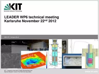
WP6 meeting
This document outlines the procedures for High-Intensity Chip (HIC) assembly, focusing on laser soldering and chip placement on a vacuum table. Key steps include positioning checks, alignment, SnAg ball deposition, and thorough soldering verification. The assembly process emphasizes efficient module production, highlighting the potential for automation through artificial vision systems. The document also details the planning of HICs assembly with module specifications, timing hypotheses, and collaboration scenarios with institutions like CERN and INFN+NIKHEF.


WP6 meeting
E N D
Presentation Transcript
WP6 meeting 06/08/2013
HIC assembly procedure Laser soldering • Placement of chips on vacuum table and position check • Placement of flex on vacuum table • Placement of soldering grid on flex • Alignment • SnAg balls deposition and check • Soldering of one chip • Repeat steps 5 and 6 for all chips • Soldering check • Final check of chips position Chips embedding • Placement of chips on adhesive support and position check • PCB workshop sequence: pressing, coverlay, holes by etching, metallisation, lines by etching, coverlay, holes by etching metallisation, lines by etching, coverlay • Final check of chips position
HIC assembly procedure General requirements • Placement of chips and position measurement with 5-10 mm resolution • Produce one module/day: automatize when possible repetitive tasks (not clear with embedding technique) • Laser soldering tasks which could be automatized using artificial vision based system: • Placement of chips on vacuum table and position check • Alignment of chips, flex, soldering grid • SnAg balls deposition and check (balls loading not clear yet) • Soldering of chips • Soldering check • Final check of chips position
Planning of HICsassembly • Inner barrel • 48 staves x 2 + 10% ~ 110 staves • 990 chips, 49500 solderings • Outer barrel • 1602 modules +10% ~ 1800 modules • 25200 chips, 1260000 solderings
Planning of HICsassembly Assembly timing hypothesis: • Placement of chips on vacuum table (auto): 9x10” ~ 90” (14 chips: 140”) • Placement of flex on vacuum table + grid on flex (man, pinholes): 300” • Alignment (auto): 300” (in parallel: manual loading of balls pick-up tool?) • SnAg balls deposition + soldering of one chip (auto): 300” + 50x 10”= 800” Total per IB module: 2h 11’ -> 30 d for full IB Total per OB module: 3h 19’ -> ~ 750 d for full OB Possible sharing scenario: • CERN -> 110 IB + 450 OB-layer 3, 4 -> 220 d • INFN+NIKHEF -> 1350 OB-layer 5, 6 -> 562 d (1 d = 8h)
VEA • VEA is a company providing artificial vision based systems for quality checks, accurate positioning, etc…, with the required precision • A system with one robotic arm to pickup objects and an X-Y movement of the laser head could do the job • VEA is available for consultancy, they would sell us a voucher with a given no. of hours considered sufficient to study and finalize a system proposal