Download
1 / 29
290 likes | 445 Vues
Status of FADC250s and Trigger Modules Heavy Photon Search Collaboration Meeting 18 October 2011 R . Chris Cuevas. Status update from May 2011 FADC250 and Trigger modules Two crate testing success Schedule How about those requirements? What’s happened since May-11?

E N D
Status of FADC250s and Trigger Modules Heavy Photon Search Collaboration Meeting 18 October 2011 R. Chris Cuevas • Status update from May 2011 • FADC250 and Trigger modules • Two crate testing success • Schedule • How about those requirements? • What’s happened since May-11? • Nov-11 test activities • Update firmware for Spring 2012 requirements • Summary
Trigger Hardware Status • Flash ADC 250Msps ( FADC250 ) • 40 Pre-production units received and tested • Automatic board level verification test station is complete. • CODA library ‘driver’ complete and is used in two crate DAq test station • Crate Trigger Processor ( CTP) • We have 4 fully functional CTP modules • 2 latest CTPs include FPGA that support higher Gigabit speed (5Gbp/s) • A new CTP was used for verification of new WIENER VXS backplane • FADC250-V2 Gigabit outputs verified with CTP @2.5Gb/s per lane! • Sixteen FADC250 boards successfully tested in full crate! • - Final test with two crate system imminent • Transports trigger data over fiber to Global Trigger crate (SSP) 2
Flash ADC 250MHz Fast Electronics DAQ Groups 23-Sept-2011 • 16 Channel, 12-bit • 4ns continuous sampling • Input Ranges: 0.5V, 1.0V, 2.0V • (user selectable via jumpers) • Bipolar input, Full Offset Adj. • Intrinsic resolution – σ = 1.15 LSB. • 2eSST VME64x readout • Several modes for readout data format • Raw data • Pulse sum mode (Charge) • TDC algorithm for timing on LE • Multi-Gigabit serial data transport of trigger information through VXS fabric • On board trigger features • Channel summing • Channel coincidence, Hit counters • Automatic Test Station is complete • Engineering Run – 40 Delivered! • 18 Hall D • 17 Hall B • Production Procurement FY12 (>$2M) • - 604 Boards for all Halls 3
Crate Trigger Processor H. Dong J. Wilson • Includes 3 Xilinx VirtexV FX70T that support 5Gbp/s • Crate Trigger Processor computes a crate-level energy sum (or hit pattern) • Computed crate-level value sent via 10Gbps fiber optics to Global Trigger Crate (32bits every 4ns) CTP • Fully populated front end crate for readout of 12GeV detector signals • 256 coaxial input ‘channels’ • VXS serial fabric is used to transfer trigger information forward to Global Trigger system. MTP Parallel Optics 10Gb/s to SSP VXS Connectors Collect serial data from 16 FADC-250 4
Trigger Hardware Status • Trigger Interface – Trigger Distribution ( TI - TD ) • FY11 test goals have been achieved • 10 pre-production units have been fabricated, assembled and tested • Final production quantities as follows: • -- Hall D: 56 units • -- Other Halls: 35+ units • Peripheral modules used with TI have been completed. • (i.e. Fan-out board for CAEN V1290 TDC) • CODA library has been updated for latest TI-D revision. • Successful test verification in two crate test stand • Procedure to align (de-skew fiber optic length differences) has been completed and verified with two crates in the lab. 5
Trigger Hardware Status - TI W. Gu DAQ Group 23-Sept-2011 ‘Legacy’ Trigger Supervisor Interface • Direct link to Trigger Supervisor crate via parallel fiber optic cable • Receives precision clock, triggers and sync from TD • Connects directly to SD on VXS backplane • Board design supports both TI and TD functions, plus can supervise up to eight front end crates. • Manages crate triggers and ReadOut Controller events TI Mode One Optical Transceiver HFBR-7924 Xilinx VirtexV LX30T-FG665 VXS P0 TD mode: from SD TI/TS mode: to SD External I/O (trg, clk…) Trigger Interface “Payload Port 18” 6
Trigger Hardware Status - TD W. Gu DAQ Group 23-Sept-2011 ‘Legacy’ Trigger Supervisor Interface • Distributes from Trigger Supervisor crate to front end crates (TI) • Distributes precision clock, triggers, and sync to crate TI modules • Board design supports both TI and TD functions, plus can supervise up to eight front end crates. • Manages crate triggers and ReadOut Controller events TD Mode Eight (8) Optical Transceiver HFBR-7924 Xilinx VirtexV LX30T-FG665 VXS P0 TD mode: from SD TI/TS mode: to SD External I/O (trg, clk…) Trigger Interface “Payload Port 18” 7
Trigger Hardware Status • Signal Distribution ( SD ) • 6 Pre-production boards have been manufactured, assembled and passed acceptance testing. • SD provides precision low jitter fan-out of 250MHz system clock, trigger and synch signals over VXS backplane to VXS payload modules • Latest SD version includes clock jitter attenuation PLL • 2 pre-production boards are installed and running in the two crate test station • Production procurement has been moved to FY12 • Quantity of 80 SD boards for all Halls 8
N. Nganga 23-Sept-2011 Crate Level – Signal Distribution (SD) • Jitter attenuation circuitry has achieved ~1.5ps rms measured at FADC250 module • All SD functions have been tested • -Synchronization • -Token Passing • -Busy signal management • SD boards have been used in the two-crate tests since the beginning of Summer 2011 without glitches. • PCB manufacture and Board assembly was ~$1000 per board • SD components are estimated at $1200 per board (price break dependent). Altera FPGA Cyclone III VITA 41 Switch Slot Connectors VXS Switch Module 9 14
Trigger Hardware Status • SubSystemProcessor ( SSP ) • Prototype board has been tested and is ahead of schedule. • New applications have been proposed for the SSP (CLAS12) • SSP is in use for two crate DAq testing • Firmware to handle trigger information from two CTP streams is complete • SSP will collect trigger data from the two full crates and deliver the final trigger signal to the Trigger Interface. • SSP to GTP serial link definitions have been fully specified and implemented for VXS • Initial testing of SSP (Xilinx) => GTP (Altera) Gigabit transceivers is successful • Manages trigger information from up to 8 front end crates. • (2048 channels!) • Trigger data received on front panel with fiber transceivers • 10Gbp/s input capability ( 4 lanes @3.125Gbp/s*(8/10b) ) • 10Gpb/s output stream to GTP on VXS backplane 10
Ben Raydo 9-Sept-2010 Sub-System Processor VME64x (2eSST support) VXS-P0 (up to 16Gb/s to each GTP) Optional DDR2 Memory Module (up to 4GByte) 2x NIM (bidirectional) 4x ECL/PECL/LVDS In 4x LVDS Out 8x Fiber Ports --10Gb/s each from CTP ) Collects Trigger Information from 8 Front End Crates 11
Trigger Hardware Status • Global Trigger Processor ( GTP ) (FY – 11/12) • 1st Article GTP module has been fabricated, assembled and received • The initial acceptance test plan is presently being executed and further testing will be completed soon. • Interface requirements to SSP and TS have been finalized • The GTP transceivers (Altera) have been tested with the SSP transceivers (Xilinx) over the VXS backplane without problems • Significant amount of firmware development and verification activity remains: • Ethernet interface • Implementation of final Physics Trigger equations • Full test of Global Trigger Crate planned for last quarter of FY12 12
GLOBAL TRIGGER PROCESSOR1st Article Board S. Kaneta 2011 Gigabit Links to SSP VXS “Switch” card DDR2 Memory 256 MB 4 Channel Fiber RJ45 Ethernet Jack Altera FPGA Stratix IV GX 4x 8-Channel LVPECL Trigger Outputs to TS 13
Trigger Hardware Status • Trigger Supervisor ( TS ) (FY-11/12 activity) • William Gu has completed the schematic and board layout • Design review planned before 1st article order • Order is scheduled for first quarter of FY12 • Test plans include functional hardware verification with TD and GTP modules • New board format from legacy era – VXS Payload module • Distributes precision clock, triggers, and sync to front end crates via the Trigger Distribution modules. • Manages global triggers and ReadOut Controller events • Global Trigger Processor drives 32 bit trigger word to TS over copper cables. • Specification has been updated to match GTP output 14
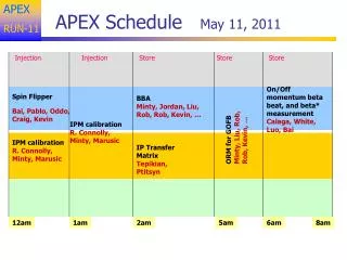
Two crate Trigger Signal From SSP to TI(TS) CODA 150m fiber through MTP patch panel LINUX Dell 2GHz Xeon Dual core 1U “DSC8” Ethernet 50m fiber through MTP patch panel Network Switch LINUX “DSC9” Two DAQ Crate Testing: FY11 15 22
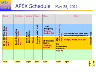
Two DAQ Crate Testing: FY11 • Pre-Production and 1st article • boards have been received and tested • Significant effort for circuit board • fabrication, assembly and acceptance • testing • System testing includes: • Gigabit serial data alignment • 4Gb/s from each slot • 64Gb/s to switch slot • Crate sum to Global crate @8Gb/s • Low jitter clock, synchronization • ~1.5ps clock jitter at crate level • 4ns Synchronization • Trigger rate testing • Readout Data rate testing • Bit-Error-Rate testing • -Need long term test (24 - 48 hrs) • Overall Trigger Signal Latency • ~2.3us (Without GTP and TS) 200KHz Trigger Rate! Readout Controller Capable of 110MB/s - Testing shows we are well within limits 16
Discussions at the May 2011 meeting,, • Define requirements for readout electronics and trigger hardware • Expected signal rates - Has this been determined from simulation for the Spring 2012 test? • Expected signal amplitudes/pulse widths – I believe we have what we need for this. • Expected trigger rates – In Spring 2012, presumably CLAS rates will be used, correct? • Calorimeter APD channels only? Or are there Hodoscope channels? • We have 256 channels for the Nov-2011 test, so signal selection is up to the collaboration. • Channel sum resolution 6 bits proposed. Is this acceptable? • We can use the Crate Trigger Processor (Energy Sum) output as part of the trigger for the • upcoming Nov-11 test. • The firmware development has not started for the scheme proposed at • May-11 collaboration meeting 17
Flash ADC ImplementationCluster Finding with Energy Resolution/Channel [May 2011] CH-1 12 Bits 12 Bits VXS Gigabit serial fabric Transfer rate of 4Gb/s per board (2 full duplex lanes @2.5Gb/s) Use 32ns ‘window’ to Transfer 16-bytes Each channel is 1 byte: 6 bit Sum + 2 bits for clock recovery 6 bit Sum (Truncated) Every Channel To Crate Trigger Processor (VXS Switch Card) Xilinx FPGA Trigger Function Pre-Processing APD Signals 16 Bytes in 32ns Meets the 4Gb/s transfer bandwidth Per board CH-16 2 bit clock encoding Allows 8ns clock recovery in 32ns ‘window’ 6 Bit Sum 6 Bit Sum CE1 CE1 CE0 CE0 CH-1 CH-16 32 ns CH-16 CH-1 Global Trigger Round Trip Latency <3us Energy & Time Algorithms VME Readout 8μs ADC Sample Pipeline 18
Discussions at the May 2011 meeting,, • Firmware development can begin once requirements are complete. • For Spring 2012 goals: • - Must create realistic work plan for firmware on FADC250, CTP and SSP • - Plan must account for firmware simulation and testing • Hardware Status • - We have VXS crates, Crate Trigger Processors, SubSystem Processor, Trigger Interface • Signal Distribution and Read-Out Controllers • Pre-production of FADC250 have been verified • Pre-production of TI-TD, SD have been verified • All boards work in concert at 200kHz trigger rate • Delivery of production FADC250 boards should arrive by Jan-12 • Pre-commissioning (We are prepared for Spring,) • - Hall Installation activities: • =Cabling, VXS crates and readout module setup/configuration • =System level testing/troubleshooting 19
Crate Trigger Processor Point of ViewCluster Finding with Energy Resolution/Channel Sub-System Processor Serial Stream Board 1 4 x 2.5Gb/s fiber links From crates to Sub-System Processor Final Cluster Algorithm To process all calorimeter channels Cluster Energy Trigger Will have much more resolution than initial DVCS implementation Crate Trigger Cluster Combiner 8Gb/s APD Signals Serial Stream Board 16 6 Bit Sum 6 Bit Sum CE1 CE1 CH-1 CH-1 CE0 CE0 32 ns 32 ns 6 Bit Sum 6 Bit Sum CE1 CE1 CH-16 CH-16 CE0 CE0 8Gb/s 20
Summary • Pre-production Flash ADC-250 boards have been received and tested • Production procurement for contract manufacturing FADC250 boards in progress • Single board acceptance testing and full crate testing activities are virtually complete • These test activities has produced essential diagnostic tools for commissioning • Software (CODA) drivers and initialization routines have been developed • We have the required trigger modules for a full two crate system • SD VXS Signal Distribution board • TI Trigger Interface board • CTP Crate Trigger Processor board • SSP Sub-System Processor board • Plenty of VXS crates on site • We will install a single crate with sixteen FADC250 in Hall B before the end of Oct-11 • Plan is to instrument the Inner Calorimeter for readout with beam in November • Parasitic DAq operation during HD-Ice experiment • Spring 2012 Test Requirements, Firmware development, and installation work plans need to be detailed 21
Backup Slides All sorts of good stuff
Flash ADC Implementation To trigger logic Trigger Pulse Pre-Processing Capture Window Readout Energy & Time Algorithms Sample Clock Event #2 Event #1 detector signal FADC 8μs ADC Sample Pipeline Trigger Input Trigger #1 Trigger #2 • Sampling Flash ADC stores digitized signal in 8us memory • Trigger input copies a window of the pipeline and extract pulse charge and time for readout • Trigger output path contains detailed information useful for cluster finding, energy sum, etc. • Hardware algorithms provide a huge data reduction by reporting only time & energy • estimates for readout instead of raw samples 21
Flash ADC ImplementationEnergy Sum Trigger Example CH-1 12 Bits 12 Bits VXS Gigabit serial fabric Transfer rate of 4Gb/s per board (2 full duplex lanes @2.5Gb/s Transfer 16-bit Energy Sum every 4ns Energy Sum 16 Channels To Crate Trigger Processor (VXS Switch Card) + Xilinx FPGA Trigger Function Pre-Processing APD Signals CH-16 CH-16 CH-1 Global Trigger Round Trip Latency <3us Energy & Time Algorithms VME Readout 8μs ADC Sample Pipeline 22
Synchronized Multi-Crate Readout • CTP #2 is also acting as an SSP (by summing the local crate + CTP#1 sum over fiber • A programmable threshold is set in CTP, which creates a trigger when the global sum (6 FADC boards => 96 channels) is over threshold. • Example test with a burst of 3 pulses into 16 channels across 2 crates/6 FADC modules A 2μs global sum window is recorded around the trigger to see how the trigger was formed: Example Raw Event Data for 1 FADC Channel: B. Raydo
Synchronized Multi-Crate Readout Rates • FADC event synchronization has been stable for several billion events @ ~150kHz trigger rate. • Have run up to 140kHz trigger rate in raw window mode, up to 170kHz in Pulse/Time mode. • Ed Jastrzembski has completed the 2eSST VME Interface on FADC allowing ~200MB/s readout Single Crate 12 signals distributed to four FADC250 18% Occupancy B. Raydo
JLab Hall B 6 GeV DVCS Trigger Implementation B. Raydo • 424 channel Inner Calorimeter with APD readout • APD amplified signal is split to drive Discriminator, and QADC • Dual Discriminator output to drive TDC and CAEN 1495 logic modules • Discriminator pulse widths are 40ns • CAEN 1495 used for each quadrant trigger • and for combining the quadrants to form the final trigger. • CAEN 1495 boards run as 5ns state machines, and sample 424 discriminated signals every 15ns to determine hit crystals • Signals that pass Threshold are used in Quadrant Cluster Detection Algorithm to locate hits on a 3 x 3 window for all adjacent crystals • Final CAEN 1495 combines Quadrant information and compares against a programmable cluster count threshold to determine final trigger Beam View 10
JLab Hall B 6 GeV DVCS Trigger Implementation B. Raydo • Very successful operation of new trigger algorithm based on commercial discriminators and logic boards. • FPGA firmware developed on CAEN 1495 format and quadrant plus main trigger algorithms met specified cluster algorithm requirements. • Single threshold energy resolution • Programmable trigger on 1-31 detected clusters • Programmable cluster definitions • Programmable Mask for channel inputs • Fast (5ns) logic with total trigger transition delay <70ns DVCS Cluster Finding Display 11