Download
1 / 1
130 likes | 598 Vues
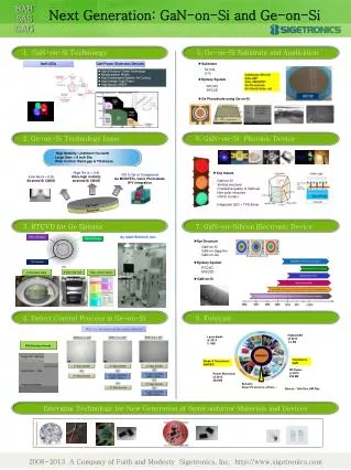
Way to minimize dislocation density. GaN LEDs. GaN Power Electronic Devices. GaN&SiC. Next Generation: GaN-on-Si and Ge-on-Si. GaN HEMTs in RF telecommunications. GaN-on-Si Technology. 5. Ge-on-Si Substrate and Application. ▶ Substrate. Si(100), (111). High Efficiency: Green Technology

E N D
Way to minimize dislocation density GaN LEDs GaN Power Electronic Devices GaN&SiC Next Generation: GaN-on-Si and Ge-on-Si GaN HEMTs in RF telecommunications • GaN-on-Si Technology 5. Ge-on-Si Substrate and Application ▶Substrate Si(100), (111) • High Efficiency: Green Technology • Miniaturization: Mobile • High Temperature Stability: Air Cooling • High Voltage: High Power • High Speed: HP&HF ▶Epitaxy System RTCVD RPCVD ▶Ge Photodiode using Ge-on-Si 2. Ge-on-Si Technology Issue 6. GaN-on-Si Photonic Device High Mobility: >2,000cm2/Vs Ge/Si Large Size: > 8 inch Dia. Wide Control: Band-gap & Thickness High Ge (x > 0.4) Ultra-high mobility strained Si CMOS ▶Key Issues 100 % Ge or Compound Ge MOSFETs, GeOI, Photodiode III-V integration Low Ge (x < 0.4) Strained Si CMOS GaN-on-Si Vertical structure Crystalline quality of GaN epi Non-polar structure Ohmic contact Integrated LED + TVS Zener Epi Layer Substrate 3. RTCVD for Ge Epitaxy 7. GaN-on-Silicon Electronic Device By SIGETRONICS, INC. 기존 6 인치 wafer 변환 8 인치 wafer ▶Epi Structure GaN-on-Si GaN-on-Sapphire GaN-on-Ge Stressed GaN-on-Si ▶Epitaxy System SiC Susceptor RTCVD MOCVD 8 inch Load Lock Temp. control system 8 inch Wafer Hand ▶GaN-on-Si 4. Defect Control Process in Ge-on-Si 8. Forecast Hybrid LED @ 2012 7.4 B$ Laser diode @ 2012 2.1 B$ PIN Structure Growth N-type Ge (~400 nm) Transistors GaN Diode & Transistors GaN/SiC RF Power @ 2012 230 M$ Intrinsic Ge (~ 3 ㎛) Power Electronic @ 2012 264 M$ Sensors Deep UV sensors, others… P-type Si substrate Source : Yole Dev, ABI Res Emerging Technology for New Generation of Semiconductor Materials and Devices