Download
1 / 22
220 likes | 335 Vues
This document outlines the research and development goals for the readout electronics of the LC Muon Detector. Short-term objectives focus on establishing a front-end system to study prototype modules, while long-term goals aim to design robust electronics for future detectors. Key issues addressed include multiplexing fibers, achieving low noise rates, optimizing time-of-arrival determination, and enhancing pulse height measurement accuracy. Various electronic components and methodologies utilized in designing the system, such as PMT integration and digitization options, are also discussed.

E N D
Readout Electronics Development for the LC Muon Detector Mani Tripathi Britt Holbrook (Engineer) Juan Lizarazo (Physics student) Yash Bansal (EE student) University of California, Davis ALCPG04 SLAC 01/07/2004
R&D Goals • In the short term, provide a front-end and readout system capable for fully studying the prototype modules being developed by the Scintillator-based Muon System group. • In the long term, develop electronics system design to be used in Muon detector at a fuutre LC.
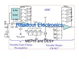
Issues to be Addressed • Multiplexing several fibers in one PMT channel • - Cost-saving is the driving force. • - Besides multiplexing physically distant fibers into one • channel of the PMT, time-separation can be also achieved • due to different lengths of clear fiber in separated channels. • - Hence, desirable to have two pulse resolution of O(5 ns). • 2. Noise rate in Multi-anode PMT at 1.5 p.e. threshold • - Acceptable singles rate to be determined based ghosting • issues encountered in #1 above. • - Expected dark rate is low (<500 p.e./s). Electronics noise • should be kept well below this.
Issues (Contd.) 3. Optimum resolution in time-of-arrival determination - O(1ns). If TOF measurement is desirable (for exotic weakly interacting heavy particles), we will need to consider improving the resolution. However, timing jitter in WLS fiber is expected to dominate. - The electronics should be able to record <1 ns in order to study the properties of scintillator + WLS. 4. Optimum resolution in pulse height/photon counting - 6-8 bit digitization with Gsamples/s can be easily achieved. If 12 bits are required for calorimetry, it can be implemented, albeit, at 100 Msps. - The latter obviously degrades two pulse resolution.
Signal Considerations Single p.e. Response: Using the typical gain and rise-time characteristics and a triangular approximation, 1 p.e. = [(4 x 106) * (1.6x10-19 C)/(0.6 ns)] *(50 W) = 53 mV Preamp response (gain of ~3-4) = 200 mV @ a rise-time of 0.6 ns = 50 mV @ a rise-time of 2.4 ns
Front-end Electronics: System Schematic +V High Gain Output I DC Pre-amp Variable Splitter PMT Low Gain Output Co-ax cable Low-Pass Filter PMT base-board Anode Current Monitoring Voltage Sensing Amp • The Pre-amp is powered by IDC from the Amp which also measures the anode current. • The co-ax cable is expected to be <100’ long, for minimizing signal loss.
Inexpensive RF amplifiers • Manufactured by Mini Circuits. The cost per chip is ~ $1.50 • Ideal for remote sensing because d.c. power is supplied on the same co-ax that carries the signal pulse.
PMT base-board/Preamplifier Layout Signal Outputs (total 16) HV Dynode resistor chain and capacitors Monolithic wide-bandwidth preamplifiers
Pre-amp Board housing 16 channel PMT and Amplifiers • 4.5” x 4.5” • Dynode resistor chain built-in • 16 amplifier chips on-board • 4 through holes on the corners for mounting.
MAPMT test-stand Bias-board PMT/Pre- amp Board LED Pulser Mounts With 90o Calibrated Rotation Dark-box
White LED for simulating noise/light-leak Fast LED pulser with collimator
Fast LED pulser with ns rise-time Plug-in LED On-board Crystal or external clock option Intensity Control via External Bias Voltage
Response of the Amplifier to a test-pulse Output in Next channel (x-talk) Output (gain~3) Input 5 ns
Post-Amplifier Response Second stage restores the signal polarity. OUTPUT INPUT The amplifier reproduces the input pulse shape faithfully => the inherent rise-time of the amplifier is better than 1 ns.
Signal Digitization Issues • Starting Points were: • Time of arrival measurement with O(1 ns) resolution. • - For the prototype system it is best achieved by utilizing • CAMAC TDCs (LRS 3377) available at Fermilab. These • modules provide 0.5 ns resolution with O(8 ns) two pulse • separation. • Pulse height measurement with O(10 bit) resolution. • - Commercial chips are available and will be utilized. However, • they work at 120 Msps and hence, one output of the amps will • need to be shaped to ~100 ns for good sampling. • - However, for the prototype system we can also use time over • threshold measurements using the TDC readout.
TDC Readout Schematic Fast Output Leading Edge Discriminator TDC From Preamp Variable Splitter Trailing Edge TDC Discriminator Slow Output ECL Control Lines ECL Data Bus LINUX PC Xilinx XCV1000 FPGA Parallel Port
General purpose FPGA board developed at UCD and used in TDC Readout ECL-LVDS Boards added Interface to Parallel Port
Future Implementation of Digitizers ADC Selection chart (Maxim-IC)
Digitizer Choice • The faster digitizers offer 1.5 Gsps @ 8-bits and can accomplish both TOA and pulse-height measurement. • The somewhat slower ones offer 1 Gsps and only 6-bits but are much cheaper (~$18/channel -- cost for 8-bit versions is >$100/channel). • The 120 Msps model @ 10-bits is much cheaper ($10/channel) but it will not have adequate time-of-arrival resolution and will require a second output for TDCs. A choice will be made in 2004 based on simulations and first measurements from scinitillator prototypes.
Summary • Amplification system for 16-channel PMT has been developed. Prototypes of post-amplifiers will be produced in 2004 • Another version of the base-board for 64-channel PMTs will be developed by summer 2004. • A DAQ for TDC modules has been developed for the test-stand. Will be installed at Fermilab in 2004. • A digitization and acquisition system is being designed for implementation in 2005.