Download
1 / 28
280 likes | 473 Vues
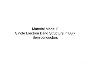
Material Model 2 Single Electron Band Structure in Bulk Semiconductors. Single Electron in Bulk Semiconductors. The Schr Ö dinger’s equation in its general form:. The Hamiltonian in semiconductors:. 1 st term – electron kinetic energy, 2 nd term – lattice ion kinetic

E N D
Material Model 2Single Electron Band Structure in Bulk Semiconductors
Single Electron in Bulk Semiconductors The SchrÖdinger’s equation in its general form: The Hamiltonian in semiconductors: 1st term – electron kinetic energy, 2nd term – lattice ion kinetic energy, 3rd term – Coulomb potential among electrons, 4th term – Coulomb potential among electrons and lattice ions, 5th term – Coulomb potential among lattice ions
Single Electron in Bulk Semiconductors Since the Hamiltonian is not explicitly time dependent, we find: Simplification of the Hamiltonian: step-1, the Born-Oppenheimer approximation (i.e., to ignore lattice ion self-effects); step-2, the Hartree self-consistent model (i.e., to count in the Coulomb effect successively rather than simultaneously);
Single Electron in Bulk Semiconductors If the n_th electron wave function is solved as: What is the wave function for a collection of N electrons? Incorrect form Correct form due to Slater step-3, the Hartree’s model must be modified to take Hartree-Fock’s form (i.e., to count in the electron spin effect):
Single Electron in Bulk Semiconductors • Solution techniques • The pseudo-potential method (Physicists’ method) • The tight-binding method (Chemists’ method) • The k-p method (for direct bandgap material at its band structure extremes and neighborhoods) • We will focus on the k-p method only in dealing with the material optoelectronic property for compound semiconductors • Otherwise, we have to rely on, e.g., the pseudo-potential method
Single Electron in Bulk Semiconductors Following the k-p method, we can rewrite the Hamiltonian as: with a most important feature that describe the electron behavior inside bulk semiconductors: It is this feature that leads to Bloch’s theorem:
Single Electron in Bulk Semiconductors Instead of the original equation (only one) for electron wave function which is defined in the entire crystal bulk, this equation for the lattice wave function is defined in a primitive cell. There are, however, N1N2N3 such equations, for all possible k values, which is also consistent with the total number of primitive cells inside the bulk crystal. Why bother then?
Single Electron in Bulk Semiconductors Conceptually, the electron E~k relation shows partially almost continuous, partially discrete, hence we have the famous electronband structure for semiconductors. Why the eigen value (energy) shows the band structure? It can be seen from the spectrum of the lattice wave function that satisfies:
1st BZ Energy band (continuous as N10) G -b1/2 0 b1/2 k Energy band gap Energy band (continuous as N10) b1/N1 G 0 k -b1/2 b1/2 0 -b1/2 b1/2 b1/N1
Single Electron in Bulk Semiconductors • Why discontinuities on E~k curve must happen at the Brillouin zone (BZ) edges? • At discontinuities, E must take its extreme at least along one direction in k-space. • Motion of electron in bulk semiconductors – partially free and partially bounded, the former reflects the property of the free-space occupied by the whole bulk, the latter reflects the property of the periodic structure (semiconductor lattice) • The expanded BZ and the reduced BZ, the reason we adopt reduced BZ description.
E Electron in 1D lattice (energy bands appear) Bands with positive effective mass Reduced BZ Electron in free space (continuous energy in parabolic shape) Conduction bands (empty at 0K) Bands with negative effective mass Valence bands (filled up with electrons at 0K) 0 k … … 4th BZ 3rd BZ 2nd BZ 1st BZ 2nd BZ 3rd BZ 4th BZ Extended BZ
Single Electron in Bulk Semiconductors • The free space – electrons have continuous E~k relation, hence limit themselves to one type, multiple states; easiest for transport, not possible for discrete transitions; easy to access but limited useful property to offer; applications include: vacuum tube transistor, microwave traveling wave amplifier, etc. • Atomic, molecular, or ionic systems – electrons have discrete E~k relation (discrete energy levels), hence limit themselves to multiple type, single states; easiest for excitations and transitions, hard for transport; useful property to offer but hard to access; application include: lasers, masers, etc. • Bulk semiconductors – electrons have partially continuous partially discrete E~k relation (energy bands), hence they are in multiple type and multiple states; easy for both excitations or transitions and transport; useful property to offer and easy to access; a variety of applications
Single Electron in Bulk Semiconductors • Major drawback of bulk semiconductors compared to the atomic, molecular, or ionic systems – intra-band electron interactions • Ideal solution – low dimension semiconductor structures, i.e., quantum wells, quantum wires, and quantum dots; e.g., similar to the atomic system, QD has discrete energy levels, hence it has all the merits possessed by the atomic system; when combined with the bulk semiconductor, it also becomes accessible; it is this feature that makes the low dimension semiconductor structures (e.g., QD) so attractive!
Single Electron in Bulk Semiconductors Step-1 Kane’s model If k=0 The radial dependence follows the Laguerre polynomials. The angular dependence follows: Spherical harmonic function Legendre function
Single Electron in Bulk Semiconductors n=1,2,3,… (known as the total quantum number) l=0,1,2,…,n-1 (known as the angular quantum number, which corresponds to s, p, d, f,… orbits) m=-l,-l+1,…,-1,0,1,…l-1,l (known as the magnetic quantum number) ms=-1/2,1/2 (known as the spin quantum number) Therefore, a bound electron by the lattice ion, similar to the orbiting electron in H-atom, is described by a set of quantum numbers: (n, l, m, ms).
Single Electron in Bulk Semiconductors , The first few orbits (electron eigen states) are given as:
Single Electron in Bulk Semiconductors , Under these states, the Hamiltonian is diagonalized as: Considering the spin of electrons, but ignoring the spin-orbiting interaction, we have: under:
Single Electron in Bulk Semiconductors , , However, the spin-orbiting interaction is not negligible in calculating the semiconductor band structure. We have to include this interaction by modifying the Hamiltonian to: Replacing p by p+ħk, we obtain the equation for the lattice wave function again (with spin-orbiting interaction included):
Single Electron in Bulk Semiconductors , It is easy to prove that, under the reordered base: we have: where:
Single Electron in Bulk Semiconductors , Following a standard perturbation procedure to diagonalize the Hamiltonian, we find that under the electron state: the Hamiltonian becomes:
Single Electron in Bulk Semiconductors , The other half of the state is: Hence, the full Hamiltonian becomes:
Single Electron in Bulk Semiconductors , Final result of Kane’s model: Conduction band Heavy hole band Light hole band Spin-orbit split band
Single Electron in Bulk Semiconductors Step-2 Luttinger-Kohn’s model Rewrite the equation for the lattice wave function as: Following the Lowdin’s renormalization theorem and taking the Kane’s solution at k=0 for valence bands, we write:
Single Electron in Bulk Semiconductors Hence we obtain:
Single Electron in Bulk Semiconductors Once the above eigen value problem is solved (a 6-order polynomial equation root-searching problem), we find valence bands as: subject to:
Single Electron in Bulk Semiconductors For conduction bands, we write: We obtain the solution in closed form:
Single Electron in Bulk Semiconductors By ignoring spin-orbit split bands and the small anisotropy in x-y plane, we may reduce the 6 6 Hamiltonian to 4 4. Hence a closed form for valence bands is obtainable as:
Single Electron in Bulk Semiconductors • As a summary of this section, we give following examples on the Hamiltonian selection in k-p theory based on Luttinger-Kohn’s model. • - Two bands in group A (heavy hole and light hole) with 44 Hamiltonian: InGaAs-AlGaAs-GaAs, InGaP-AlInGaP-GaAs, InGaAsP-InP and AlGaInAs-InP [12] • - Three bands in group A (heavy hole, light hole, and spin-orbit split) with 66 Hamiltonian: InGaAsP-InP, AlGaInAs-InP and group-III nitrides with wurtzite structure such as InGaN-AlGaN [16] • - Four bands (e.g., conduction, heavy hole, light hole, and spin-orbit split) with 88 Hamiltonian: wide bandgap II-VI compounds [17], group-III nitrides with wurtzite structure such as InGaN-AlGaN [18], group-III antimonides, and narrow bandgap II-VI compounds [19] • - Five bands (e.g., N-resonant, conduction, heavy hole, light hole, and spin-orbit split) with 1010 Hamiltonian: diluted nitrides such as GaInNAs-AlGaAs-GaAs [20]