Download
1 / 26
270 likes | 466 Vues
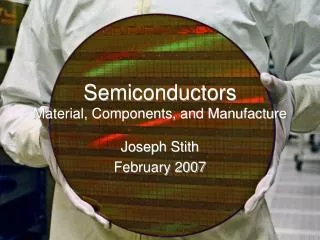
Semiconductors Material, Components, and Manufacture. Joseph Stith February 2007. Outline. Atom Electron Energy Levels Electrical properties of materials Doping Diodes Capacitors Transistors High-K dielectric / Metal Gate Flash Transistor Manufacturing Process

E N D
SemiconductorsMaterial, Components, and Manufacture Joseph Stith February 2007 Stith
Outline • Atom Electron Energy Levels • Electrical properties of materials • Doping • Diodes • Capacitors • Transistors • High-K dielectric / Metal Gate • Flash Transistor • Manufacturing Process • Semiconductor Mfg History • Possible Futures • Intel Arizona Fabs Stith
Electron Energy Levels • Electrons collect in various regions, often referred to as Energy Levels, shells, orbitals, etc. Drawn representatively as circles. • Atoms seek stability: Full energy Levels: 2, 8, 8, … • How many electrons does this Silicon atom seek? • 4 • Where does it get the additional electrons? • Sharing outer shell electrons with other atoms that also want additional electrons, creating a bond. H20 NaCl SiO2 Stith
Electrical Properties • Insulator • No free electrons • Conductor • free electrons • Semi-Conductor • No free electrons • Insulator • But… Stith
Doping • Increases conductivity • N-Type (5 outer electrons) • Phosphorus or Arsenic • P-Type (3 outer electrons) • Boron Stith
Diode • P-Doped and N-Doped Regions • Both regions are conductors • Junction may not be a conductor Holes & Electrons flowing Depletion Region Positively Biased Stable Covalent Electrons Depletion Region Negatively Biased Holes Electrons Holes Electrons Stith
Capacitor - + - + - • Two conductors separated by an insulator • Plates charge, but no current flows through the capacitor. • Once charged, there is an electrical field between the plates. • Discharging one plate (e.g., attaching to ground) will still leave an electrical field. • Electrical field will attract opposite particles in other plate. - - + - + Stith
Transistor N P N • With no gate charge, no current. • Two reversed diodes • One capacitor • With a positive gate charge, a channel of negative ions form at the top of the P region, allowing current to flow. Stith
High-k + Metal Gate Stith
Flash Transistor • Flash memory still uses MOS Transistors for control functions. • Uses Flash transistors to store data • Floating Gate surrounded by insulator Stith
Manufacturing Process • Fab • Add material • Implant • Diffusion/Anneal • Heat raises energy of atoms to allow them to settle to a more stable location. • Thin Films • Sputter, Oxidation, Chemical Vapor Deposition • Remove material • Etch (chemical; acids): Wet (undercuts), Plasma (straight). • Planar (mechanical) • Determining the pattern/Lithography • Spin on a layer of Resist • Expose to light through pattern (negative) • Wash off the unexposed resist • Add material (below) • Wash off the exposed resist • Metrology (lot OOC, Tool OOC, Trending to OOC) • C4 • Sort • Assembly/Test Stith
1. Layer SiO2 2. Apply Resist 3. Expose Resist 4. Remove unexposed 5. Etch SiO2 5. Remove exposed 6. Layer Polysilicon gate 7. Apply Resist 8. Expose Resist 9. Remove unexposed 10. Etch Polysilicon 11. Remove exposed 12. Dope Silicon 13. Add SiO2 14. Apply Resist 15. Expose Resist 16. Remove unexposed 17. Etch SiO2 18. Remove exposed 19. Layer Aluminum 20. Apply Resist 21. Expose Resist 22. Remove unexposed 23. Etch Aluminum 24. Remove exposed Manufacturing a Transistor Gate Contact • http://micro.magnet.fsu.edu/electromag/java/transistor/index.html • http://www.tel.com/eng/product/spe/spe.htm METROLOGY Source Contact Drain Contact Stith
History Stith
Possible Futures Stith
Possible Futures Stith
Future: Multi-Core - Polaris • http://blogs.zdnet.com/OverTheHorizon/?p=12 Stith
Intel Arizona • Chandler Blvd • Offices • Assembly Test development area • Ocotillo • F22 – 8” Fab - Closing Q1 2008, F32 will grow into the floorspace as it transitions to 32nm • F12 – 12” Fab – Running 65nm – Converted from 200mm - Converting to chipset fab. • F32 – 12” Fab – Startup 45nm - $3B - 184,000 square feet of clean room space Stith
Questions? Stith
Backup Stith
Further Info • http://micro.magnet.fsu.edu/electromag/java/siliconcreature/sailboat.html • http://micro.magnet.fsu.edu/electromag/java/transistor/index.html • http://nobelprize.org/educational_games/physics/transistor/function/index.html Stith
Contamination • Class 1 clean room • 10,000 times cleaner than an operating room. • 1 particle (> .5 micron) per cubic foot of air. • FOUPs • Allow for dirtier fabs • Environment • 72 degrees Fahrenheit • 40% humidity • Positive air pressure • Assembly/Test less strict Not Allowed: Gum, perfume, makeup, pencils, standard paper Stith
Electrons Stith
http://winter.group.shef.ac.uk/orbitron/AOs/3d/index.html Stith
http://www.webelements.com/webelements/elements/text/Si/econ.htmlhttp://www.webelements.com/webelements/elements/text/Si/econ.html Stith
References • http://computer.howstuffworks.com • http://www.chemguide.co.uk/atoms/properties/atomorbs.html#top • http://www.chemguide.co.uk/index.html#top • www.webelements.com • http://www.chemguide.co.uk/atoms/bonding/covalent.html • www.sela.com/cmossem.htm • http://cache-www.intel.com/cd/00/00/33/04/330432_330432.pdf • http://en.wikipedia.org/wiki/High-k_Dielectric Stith