Download
1 / 13
130 likes | 615 Vues
Structure and Bonding in Metals. Properties of Metals high thermal conductivity high electrical conductivity malleability (metals can be pounded thin) ductility (metals can be drawn into a fine wire) durable high melting points

E N D
Structure and Bonding inMetals • Properties of Metals • high thermal conductivity • high electrical conductivity • malleability (metals can be pounded thin) • ductility (metals can be drawn into a fine wire) • durable • high melting points • Properties are due to the nondirectional covalent bonding found in metallic crystals
Structure and Bonding in Metals • Metallic Crystals • picture as spherical atoms packed together and bonded to each other equally in all directions • Closest Packing arrangement - most efficient packing in terms of using all available space • each sphere is surrounded by six other spheres • hexagonal closest packed structure - aba arrangement (spheres in the third layer are directly over those in the first layer) • cubic closest packed structure - abc arrangement (no spheres in the third layer can lie over one in the first layer)
Bonding Models for Metals • Properties of metals indicate bonding in metals is both strong and nondirectional • Strong bonding - difficult to separate atoms • Nondirectional bonding - easy to move atoms, as long as they stay together
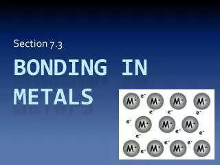
Bonding Models for Metals • Electron sea model • simplest picture • a regular array of metal cations in a sea of valence electrons • mobile electrons can conduct heat and electricity • metal ions can be easily moved around as the metal is hammered or pulled • Bonding is considered to be nondirectional covalent bonds involving delocalized electrons
Bonding Models for Metals • Band Model aka Molecular Orbital (MO) model • Electrons travel around the metal crystal in molecular orbitals formed from the valence atomic orbitals (MO theory…bonding and antibonding orbitals made from two atomic orbitals)
Bonding Models for Metals • MO theory for metals • when many metal atoms interact, the large number of molecular orbitals formed become very closely spaced in terms of energies. • These closely spaced molecular orbitals form a continuum of energy levels or bands.
Bonding Models for Metals • Core electrons are localized, fixed in place close to the metal ions • Valence electrons occupy partially filled, closely spaced molecular orbitals • Empty molecular orbitals help explain thermal and electrical conductivity.
Bonding Models for Metals • Apply a current to a strip of metal • for current to flow, electrons must be able to move freely • In the band model, electrons in filled MO’s can be excited to fill empty MO’s. • The electrons that conduct electricity occupy the MO’s known as the conduction band. • The same principle applies for heat conduction
Metal Alloys • ????????????
Semiconductors • Diamond is a nonconductor • Unlike metals, the empty MO’s are much higher in energy than the filled MO’s • It would be difficult for an electron to be excited to the empty MO’s • Silicon is a semiconductor • The gap between the filled and the empty MO’s is smaller. It is a little easier for e-’s to jump to the empty MO’s…but not as easy as for e-’s in a metal.
Semiconductors • At higher temperatures, conductivity of silicon increases. It becomes easier for e-’s to make the jump to the empty MO’s. • Enhance conductivity of silicon by doping the crystal with other elements.
Semiconductors • N - type semiconductor - dope Si with atoms with more valence e-’s (e.g. with As) • the extra electrons from As can conduct an electric current • analogy: Given a row in a movie theater filled with people. Each person has a bag of popcorn. One person has two bags of popcorn. Passing one bag of popcorn (the extra electron) down the row is like electricity being conducted in an n-type semiconductor.
Semiconductors • p-type semiconductor - dope Si with atoms with less valence e-’s (e.g. with B) • B’s three valence e- leave a hole in an MO. • Another e- could move into the hole, but it would leave another hole for another electron to fill • Analogy: In a movie theater, a row of seats is filled, except for one seat. One person could get up out of his seat and move into the empty seat. The next person could then move into the newly emptied seat, and so on… • the p in p-type refers to the positive hole formedwith a missing valence electron