### Development of an Advanced OEM PCI Board with Altera FPGA and Integrated IO Solutions ###
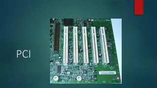
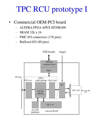
This document outlines the design and specifications of a prototype OEM PCI board featuring the Altera FPGA APEX EP20K400. It includes 32k x 16 SRAM, PMC I/O connectors with 178 pins, and buffered I/O capabilities with 80 pins. The board supports the FEE bus, facilitating effective communication with trigger boards. Moreover, it integrates internal SRAM and FLASH EEPROM for enhanced memory management. Various programming models and data paths are defined, alongside software API considerations for Linux drivers, ensuring compatibility with command decoders and mailbox protocols. ###

### Development of an Advanced OEM PCI Board with Altera FPGA and Integrated IO Solutions ###
E N D
Presentation Transcript
TPC RCU prototype I • Commercial OEM-PCI board • ALTERA FPGA APEX EP20K400 • SRAM 32k x 16 • PMC I/O connectors (178 pins) • Buffered I/O (80 pins) FEE boards trigger FEE-bus daughter board PMC PCI bus FPGA APEX20k400 PCI core Glue logic I/O SIU card internal SRAM 32k x 16 FLASH EEPROM onboard SRAM
TPC RCU prototype II SC TTC FEE-bus PCI bus Memory D32 SIU-CMC interface FPGA PCI core Glue logic 2 MB SIU card internal SRAM > 2 MB FLASH EEPROM Memory D32
RCU test system FEE-boards RCU Trigger FEE-bus SIU LINUX: DATE PCI-tools FPGA PCI bridge interface SIU SRAM PCI bus pRORC DDL DIU LINUX: DATE PCI-tools Glue logic PCI bridge interface DIU PCI bus
Programming model • Data/Command path • Message passing model • Production version FEE command (”blabla_ALTRO”, , ,) DATE PCI-tools API LINUX-driver DIU command decoder PCI core mailboxes fifos DDL protocol SIU command decoder RCU command decoder RCU SM Design phase Prototype Final version
Programming model • Data/Command path • Message passing via PCI • Development version DATE PCI-tools API LINUX-driver PCI core mailboxes fifos RCU FEE controller RCU SIU emulator SIU command decoder FEE bus DDL ALTRO Design phase Prototype Final version