8255:Programmable Peripheral Interface
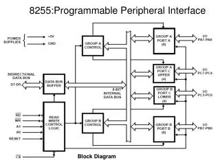
8255:Programmable Peripheral Interface. Block Diagram. Function of pins:. Data bus(D 0 -D 7 ) :These are 8-bit bi-directional buses, connected to 8085 data bus for transferring data. CS: This is Active Low signal. When it is low, then data is transfer from 8085.

8255:Programmable Peripheral Interface
E N D
Presentation Transcript
8255:Programmable Peripheral Interface Block Diagram
Function of pins: • Data bus(D0-D7):These are 8-bit bi-directional buses, connected to 8085 data bus for transferring data. • CS: This is Active Low signal. When it is low, then data is transfer from 8085. • Read: This is Active Low signal, when it is Low read operation will be start. • Write: This is Active Low signal, when it is Low Write operation will be start.
Address (A0-A1):These two lines are used to select the ports as follows:
RESET: This is used to reset the device. That means clear control registers. • PA0-PA7:It is the 8-bit bi-directional I/O pins used to send the data to peripheral or or to receive the data from peripheral. • PB0-PB7:Similar to PA • PC0-PC7:This is also 8-bit bidirectional I/O pins. These lines are divided into two groups. • PC0 to PC3(Lower Groups) • PC4 to PC7 (Higher groups) These two groups working in separately using 4 data’s.
Data Bus buffer: • It is a 8-bit bidirectional Data bus. • Used to interface between 8255 data bus with system bus. • The internal data bus and Outer pins D0-D7 pins are connected in internally. • The direction of data buffer is decided by Read/Control Logic.
Read/Write Control Logic: • This is getting the input signals from control bus and Address bus • Control signal are RD and WR. • Address signals are A0,A1,and CS. • 8255 operation is enabled or disabled by CS.
Group A and Group B control: • Group A and B get the Control Signal from CPU and send the command to the individual control blocks. • Group A send the control signal to port A and Port C (Upper) PC7-PC4. • Group B send the control signal to port B and Port C (Lower) PC3-PC0.
8255: Mode 0, Simple I/O • In this mode , port A, port B and port C is used as individually (Simply). • Features: • Outputs are latched , Inputs are buffered not latched. • Ports do not have Handshake or interrupt capability.
8255: Mode 1, Asynchronous & Interrupt Driven • In this mode, input or output is transferred by hand shaking Signals. • Handshaking signals is used to transfer data between those devices whose data transfer rate is not same. • In mode 1, Port A and Port B use the lines on Port C to generate or accept these “handshaking” signals
Mode 2 Bi-directional Operation • This functional configuration provides a means for communicating with a peripheral device or structure on a single 8-bit bus for both transmitting and receiving data (bidirectional bus I/O). • “Handshaking” signals are provided to maintain proper bus flow discipline in a similar manner to MODE 1. • Interrupt generation and enable/disable functions are also available
BIT Set Reset Mode (BSR Mode) • The PORT C can be Set or Reset by sending OUT instruction to the CONTROL registers. • The control word format for the BSR mode is shown.
FOR BIT SET/RESET MODE: • This is bit set/reset control word format. X X X Don’t care Bit select B0 B1 B2 BIT SET/RESET 1=SET 0=RESET BIT SET/RESET FLAG =0 Active